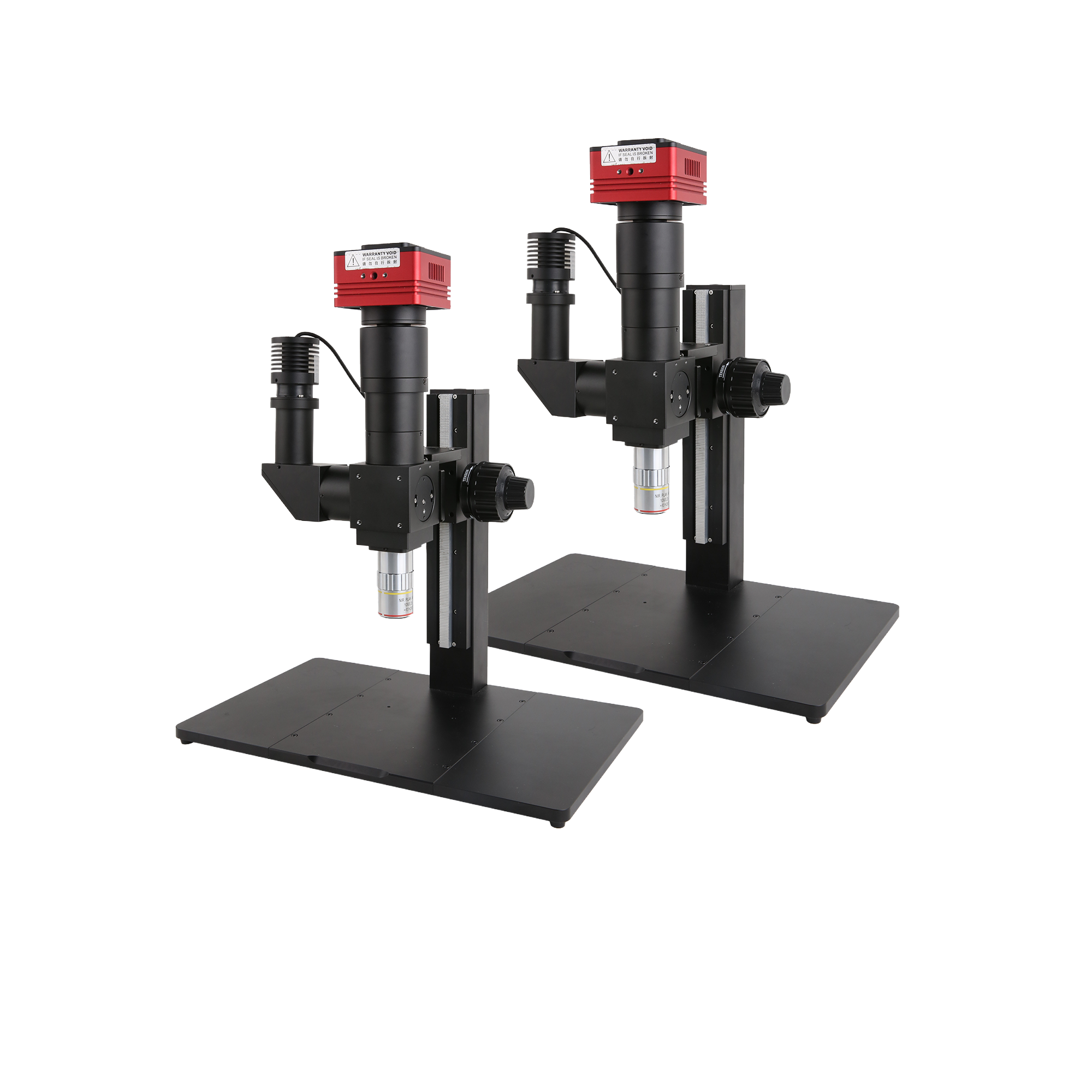


Specialised microscope systems
Product Introduction
Specialised microscope systems tailored for specific applications, spanning SWIR, differential interference contrast, brightfield metallography, fluorescence, polarisation, and more.
Product Features
- Specialised design optimised for targeted applications.
- High-quality optical components
- Modular configuration for easy expansion
- Suitable for scientific research and industrial inspection
- Comprehensive system solution
Find the right microscopy system for your application needs
Specialised microscope systems
Specialised microscope systems tailored for specific applications, spanning SWIR, differential interference contrast, brightfield metallography, fluorescence, polarisation, and more.
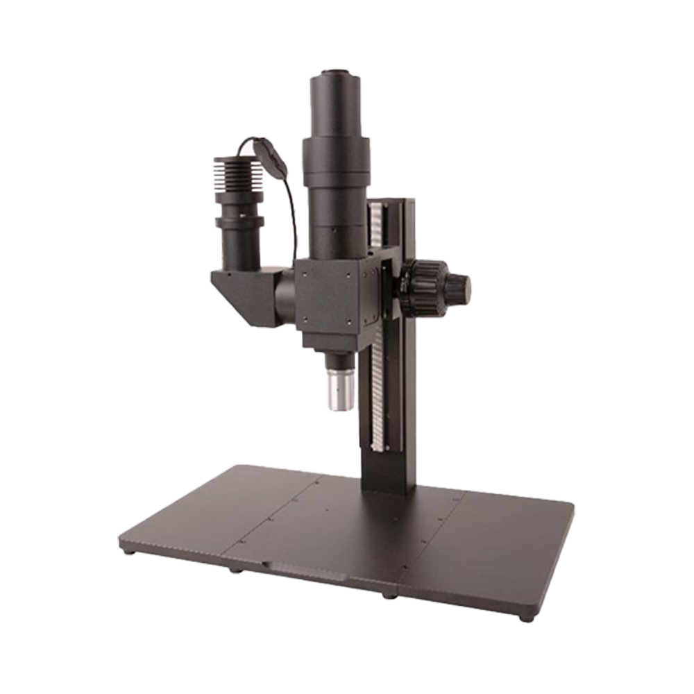
BSM - Short-wave infrared microscope system
The BSM Series SWIR modular microscope extends imaging beyond the traditional visible spectrum and into the 900-1700 nm short-wave infrared band. By c...
Main Features
- SWIR imaging range from 900-1700 nm
- Standard glass optics compatibility for easier microscope integration
- Silicon penetration capability for non-destructive internal inspection
- Modular illumination, imaging, and mechanical architecture
- Support for high NA infinity SWIR microscope objectives
- Coaxial Kohler lighting with 1550 / 1400 / 1300 / 1200 nm LED sources
- Dedicated M Plan Apo NIR objective range from 5X to 50X HR
- Micron-level resolution down to 0.4 µm with 50X HR objective
- SWIR camera options from 0.33M to 5.0M with built-in TEC
- Standard C camera interface for SWIR camera integration
- Precision CNC structure with anti-vibration design
- Scalable platform for sensor, wavelength, and automation customisation
Application Fields
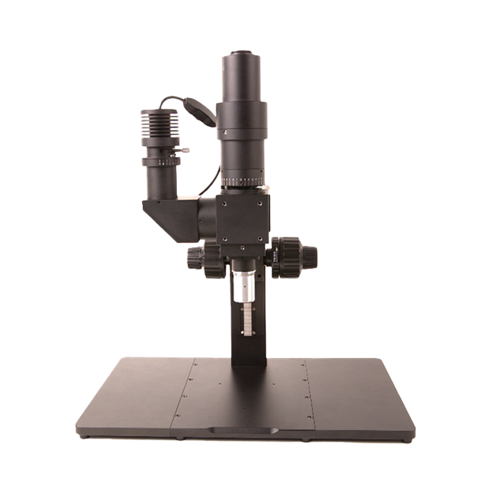
DIC100 - Differential interference contrast microscope system
The Differential Interference Contrast (DIC) microscope operates on birefringent double-beam polarisation interference:
1. Linearly polarised light fr...
Standard Working Distance Objective Parameters (45 mm parfocal distance)
| Objective Name | Magnification | Numerical Aperture | Working Distance | Focal Length | Resolution | Object Field | Image Field | Thread Size |
|---|---|---|---|---|---|---|---|---|
| DIC5XA | 5X | 0.15 | 23.5 mm | 39 mm | 2.2 µm | 5 mm | 25 mm | M26*0.705 |
| DIC10XA | 10X | 0.3 | 22.8 mm | 20 mm | 1.1 µm | 2.5 mm | 25 mm | M26*0.705 |
| DIC20XA | 20X | 0.4 | 19.2 mm | 10 mm | 0.8 µm | 1.1 mm | 25 mm | M26*0.705 |
| DIC50XA | 50X | 0.55 | 11 mm | 4 mm | 0.6 µm | 0.44 mm | 25 mm | M26*0.705 |
Long Working Distance Objective Parameters (60 mm parfocal distance)
| Objective Name | Magnification | Numerical Aperture | Working Distance | Focal Length | Resolution | Object Field | Image Field | Thread Size |
|---|---|---|---|---|---|---|---|---|
| DICL2XA | 2X | 0.055 | 33.7 mm | 100 mm | 6.1 µm | 12.5 mm | 25 mm | M26*0.705 |
| DICL5XA | 5X | 0.14 | 33.6 mm | 40 mm | 2.2 µm | 5 mm | 25 mm | M26*0.705 |
| DICL10XA | 10X | 0.28 | 33.4 mm | 20 mm | 1.2 µm | 2.5 mm | 25 mm | M26*0.705 |
| DICL20XA | 20X | 0.34 | 29.5 mm | 10 mm | 0.8 µm | 1.25 mm | 25 mm | M26*0.705 |
| DICL50XA | 50X | 0.5 | 18.9 mm | 4 mm | 0.7 µm | 0.5 mm | 25 mm | M26*0.705 |
Main Features
- Standard and long working distance objectives (optional)
- Imaging path: 1X (tube lens focal length 180 mm), optional reducers with other magnifications
- Image plane size: 25 mm
- Spectral range: 400–700 nm
- Camera interface: C-mount
- Illumination: Köhler illumination
- Light source: 10 W white LED / 3 W blue LED (optional)
Application Fields
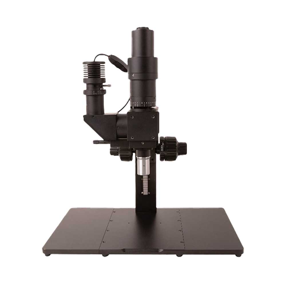
BMM100 - Brightfield metallographic microscope system
A brightfield metallographic microscope is a precision optical instrument composed of illumination, imaging, and mechanical subsystems. It is widely a...
Standard Working Distance Objective Parameters (45 mm parfocal distance)
| Objective Name | Magnification | Numerical Aperture | Working Distance | Focal Length | Resolution | Object Field | Image Field | Thread Size |
|---|---|---|---|---|---|---|---|---|
| BF5XA | 5X | 0.15 | 23.5 mm | 39 mm | 2.2 µm | 5 mm | 25 mm | M26*0.705 |
| BF10XA | 10X | 0.3 | 22.8 mm | 20 mm | 1.1 µm | 2.5 mm | 25 mm | M26*0.705 |
| BF20XA | 20X | 0.4 | 19.2 mm | 10 mm | 0.8 µm | 1.1 mm | 25 mm | M26*0.705 |
| BF50XA | 50X | 0.55 | 11 mm | 4 mm | 0.6 µm | 0.44 mm | 25 mm | M26*0.705 |
Long Working Distance Objective Parameters (60 mm parfocal distance)
| Objective Name | Magnification | Numerical Aperture | Working Distance | Focal Length | Resolution | Object Field | Image Field | Thread Size |
|---|---|---|---|---|---|---|---|---|
| BFL2XA | 2X | 0.055 | 33.7 mm | 100 mm | 6.1 µm | 12.5 mm | 25 mm | M26*0.705 |
| BFL5XA | 5X | 0.14 | 33.6 mm | 40 mm | 2.2 µm | 5 mm | 25 mm | M26*0.705 |
| BFL10XA | 10X | 0.28 | 33.4 mm | 20 mm | 1.2 µm | 2.5 mm | 25 mm | M26*0.705 |
| BFL20XA | 20X | 0.34 | 29.5 mm | 10 mm | 0.8 µm | 1.25 mm | 25 mm | M26*0.705 |
| BFL50XA | 50X | 0.5 | 18.9 mm | 4 mm | 0.7 µm | 0.5 mm | 25 mm | M26*0.705 |
Main Features
- Standard or long working-distance objective series (optional)
- Imaging path: 1X (tube lens focal length 180 mm) with optional custom reducers
- Image circle: 25 mm
- Spectral range: visible light
- Camera interfaces: C / M42 / M52 (optional)
- Illumination: critical illumination or Köhler illumination (optional)
- Light source: 10 W white LED / blue LED (optional)
Application Fields
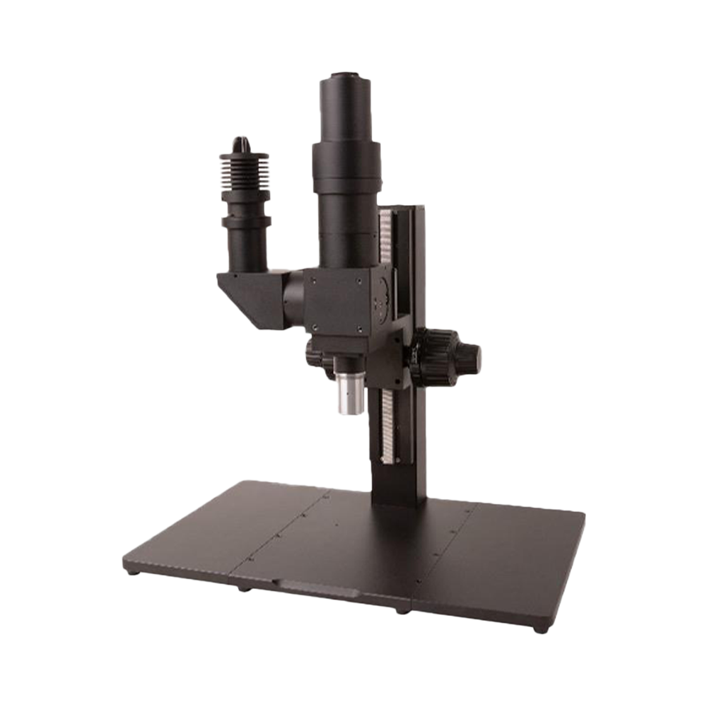
PLM100 - Professional Polarised Light Imaging Solution
A polarising microscope is designed to study anisotropic transparent or opaque materials. Substances exhibiting birefringence can be clearly distingui...
Standard Working Distance Objective Parameters (45 mm parfocal distance)
| Objective Name | Magnification | Numerical Aperture | Working Distance | Focal Length | Resolution | Object Field | Image Field | Thread Size |
|---|---|---|---|---|---|---|---|---|
| POL2.5XA | 2.5X | 0.075 | 6.2 mm | 80 mm | 4.46 µm | 10 mm | 25 mm | M26*0.705 |
| POL5XA | 5X | 0.15 | 23.5 mm | 39 mm | 2.2 µm | 5 mm | 25 mm | M26*0.705 |
| POL10XA | 10X | 0.3 | 22.8 mm | 20 mm | 1.1 µm | 2.5 mm | 25 mm | M26*0.705 |
| POL20XA | 20X | 0.4 | 19.2 mm | 10 mm | 0.8 µm | 1.1 mm | 25 mm | M26*0.705 |
| POL50XA | 50X | 0.55 | 11 mm | 4 mm | 0.6 µm | 0.44 mm | 25 mm | M26*0.705 |
Long Working Distance Objective Parameters (60 mm parfocal distance)
| Objective Name | Magnification | Numerical Aperture | Working Distance | Focal Length | Resolution | Object Field | Image Field | Thread Size |
|---|---|---|---|---|---|---|---|---|
| POLL2XA | 2X | 0.055 | 33.7 mm | 95 mm | 6.1 µm | 12.5 mm | 25 mm | M26*0.705 |
| POLL5XA | 5X | 0.14 | 33.6 mm | 40 mm | 2.2 µm | 5 mm | 25 mm | M26*0.705 |
| POLL10XA | 10X | 0.28 | 33.4 mm | 20 mm | 1.2 µm | 2.5 mm | 25 mm | M26*0.705 |
| POLL20XA | 20X | 0.34 | 29.5 mm | 10 mm | 0.8 µm | 1.25 mm | 25 mm | M26*0.705 |
| POLL50XA | 50X | 0.5 | 18.9 mm | 4 mm | 0.7 µm | 0.5 mm | 25 mm | M26*0.705 |
Main Features
- Standard and long working distance objectives available
- Imaging path: 1X (tube lens focal length 180 mm) with optional reducers
- Image circle: 25 mm
- Spectral range: visible light
- Camera interfaces: C / M42 / M52 (optional)
- Illumination: critical illumination or Köhler illumination (optional)
- Light source: 10 W white LED / blue LED (optional)
Application Fields
FM100 - Fluorescence microscope system
A fluorescence microscope observes fluorescent or phosphorescent specimens. Excitation light of a specific wavelength (or band) illuminates the sample...
Standard Working Distance Objective Parameters (45 mm parfocal distance)
| Objective Name | Magnification | Numerical Aperture | Working Distance | Focal Length | Resolution | Object Field | Image Field | Thread Size |
|---|---|---|---|---|---|---|---|---|
| BF5XA | 5X | 0.15 | 23.5 mm | 39 mm | 2.2 µm | 5 mm | 25 mm | M26*0.705 |
| BF10XA | 10X | 0.3 | 22.8 mm | 20 mm | 1.1 µm | 2.5 mm | 25 mm | M26*0.705 |
| BF20XA | 20X | 0.4 | 19.2 mm | 10 mm | 0.8 µm | 1.1 mm | 25 mm | M26*0.705 |
| BF50XA | 50X | 0.55 | 11 mm | 4 mm | 0.6 µm | 0.44 mm | 25 mm | M26*0.705 |
Long Working Distance Objective Parameters (60 mm parfocal distance)
| Objective Name | Magnification | Numerical Aperture | Working Distance | Focal Length | Resolution | Object Field | Image Field | Thread Size |
|---|---|---|---|---|---|---|---|---|
| BFL2XA | 2X | 0.055 | 33.7 mm | 100 mm | 6.1 µm | 12.5 mm | 25 mm | M26*0.705 |
| BFL5XA | 5X | 0.14 | 33.6 mm | 40 mm | 2.2 µm | 5 mm | 25 mm | M26*0.705 |
| BFL10XA | 10X | 0.28 | 33.4 mm | 20 mm | 1.2 µm | 2.5 mm | 25 mm | M26*0.705 |
| BFL20XA | 20X | 0.34 | 29.5 mm | 10 mm | 0.8 µm | 1.25 mm | 25 mm | M26*0.705 |
| BFL50XA | 50X | 0.5 | 18.9 mm | 4 mm | 0.7 µm | 0.5 mm | 25 mm | M26*0.705 |
Main Features
- Standard and long working distance objectives available
- Imaging path: 1X (tube lens focal length 180 mm) with optional reducers
- Image circle: 25 mm
- Spectral range: visible light
- Camera interfaces: C / M42 / M52 (optional)
- Illumination: critical illumination or Köhler illumination (optional)
- Illumination source: 3 W, 365 nm LED
- Fluorescence module: DAPI single-band UV filter set (365 nm excitation, 445 nm emission, 405 nm dichroic mirror), customisable
Application Fields
Special Microscopy System Features
- Specialised design optimised for targeted applications.
- High-quality optical components
- Modular configuration for easy expansion
- Suitable for scientific research and industrial inspection
- Comprehensive system solution
Selection Guide
Choose the appropriate microscopy method based on sample characteristics
Standard or long working distance objectives meet different needs
Köhler or critical illumination available
Supports C/M42/M52 and various interfaces
Topograph Photoelectric special microscopy systems adopt modular design, providing specialized solutions for different application scenarios to meet the high-end requirements of research and industrial inspection.
System Configuration Solutions
Flexibly combine hardware and software modules based on application requirements
| Dimension | Key Configuration | Technical Highlights | User Benefits |
|---|---|---|---|
| Imaging Hardware |
• ToupCam X Series: IMX415/IMX571 BSI CMOS, up to 45 MP, USB 3.0/HDMI 60 fps 4K • HCAM/PUM Portable Module: UVC plug-and-play, 8 LED ring light built-in |
• Low read noise & 66 dB+ dynamic range • Progressive scan + global shutter optional |
True color reproduction, high contrast; meets high-speed AOI, fluorescence weak signal and multi-scenario needs |
| Zoom Optics |
• MZO Series (0.25×–8×): 20× zoom ratio, NA 0.12, 174 mm long working distance • ZOPE All-in-one: Built-in 8 LED & USB camera, parfocal linear zoom |
Dual-end parallel optical path, diffraction-limited MTF, low distortion | Zoom without refocusing, view samples from millimeter to micrometer scale |
| Illumination System |
• TZM0756DRL 65/85 mm LED ring light: PWM continuously adjustable brightness • TZM0756CL coaxial light + point source • AALRL-200 large ring light: 300 mm uniform field |
Multi-channel/polarization/coaxial composite light; LED angle 30° adjustable | Solves PCB solder joint glare, wafer scratches, transparent film inspection challenges |
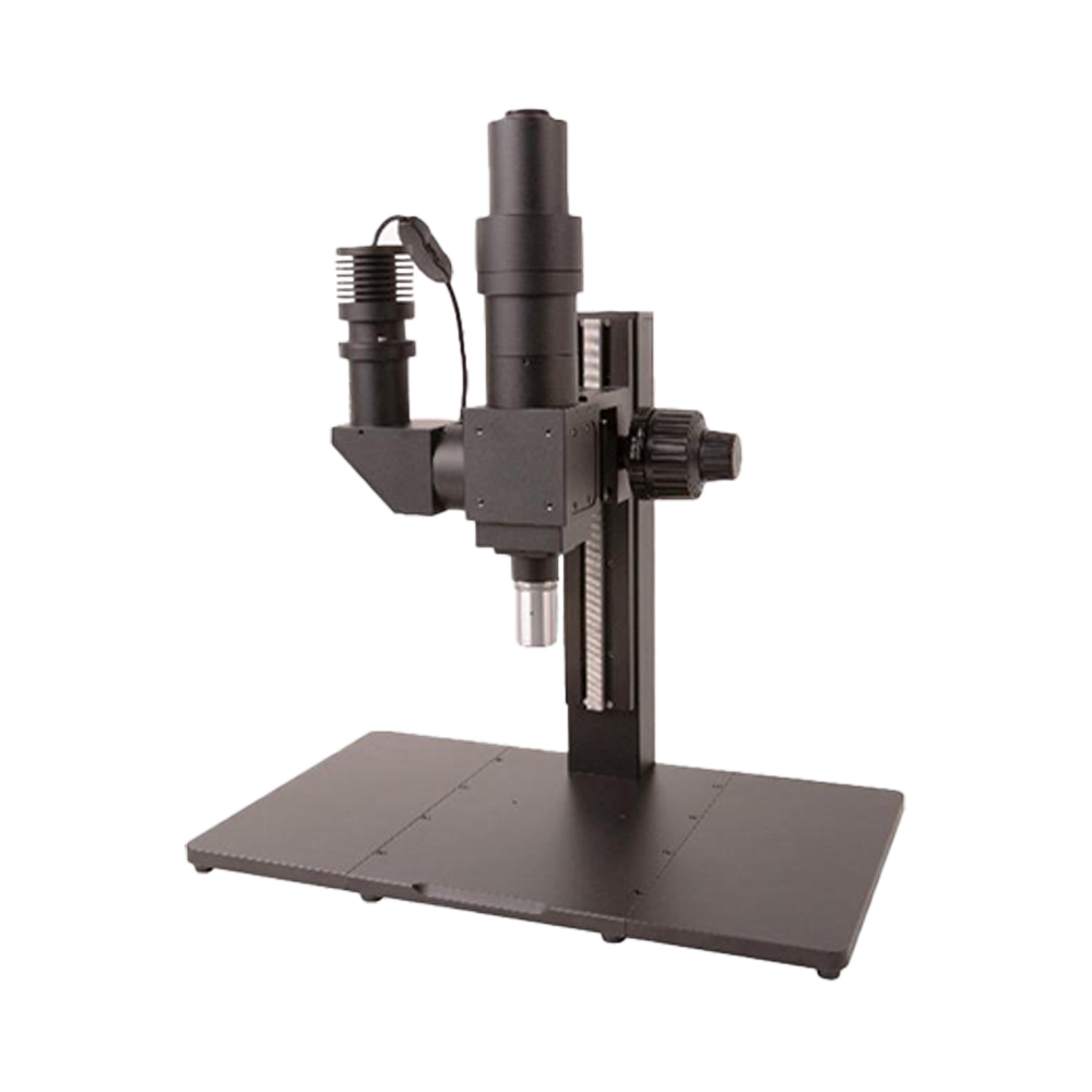
| Mechanical Platform |
• TPS-600 coarse/fine adjustment stand (5 kg load capacity) • TPS-300 precision fine adjustment 2 µm step • Motorized Z & XY platform (optional) |
Anodized Class II aerospace aluminum, ball screw | Long-term 24×7 stable positioning, supports autofocus and array scanning |
| Software & Algorithm |
• ToupView: Real-time measurement/annotation, deep focus synthesis, HDR, polarization demodulation • SDK/API: Windows/macOS/Linux/Android • AI Module: Defect classification, dimension tolerance judgment |
Secondary development + PLC/robot serial protocol | Quick integration into MES/SPC quality systems, supports edge computing and cloud synchronization |
System Advantages
Five core advantages building a professional microscopy imaging platform
Complete Ecosystem, Turnkey Delivery
All self-developed cameras, lenses, lighting, stands, and software — no multi-vendor procurement matching needed, plug-and-play saves 60% integration time.
High Resolution + Large Depth of Field
45 MP ultra-high definition CMOS + deep focus synthesis algorithm achieves micrometer-level depth clarity within a 30 mm field of view.
Multi-spectral & Low Light Imaging
Supports white light/near-infrared/polarization combination with coaxial + ring light synchronous exposure; reveals texture details even at 0.05 lux.
Flexible Expansion, Investment Protection
Standard C-Mount and GigE Vision/USB3 Vision protocols allow later upgrades to AI modules, motorized stages, and multi-camera synchronization without replacing the main unit.
Cross-Industry Implementation Cases
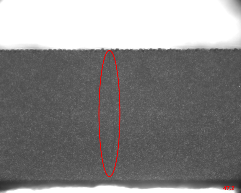
- Semiconductor: Bumping, scratch, wire bond defect AOI
- FPC/PCB: Solder paste height, pad residue detection
- New Energy: Lithium battery separator pore size, electrode coating consistency
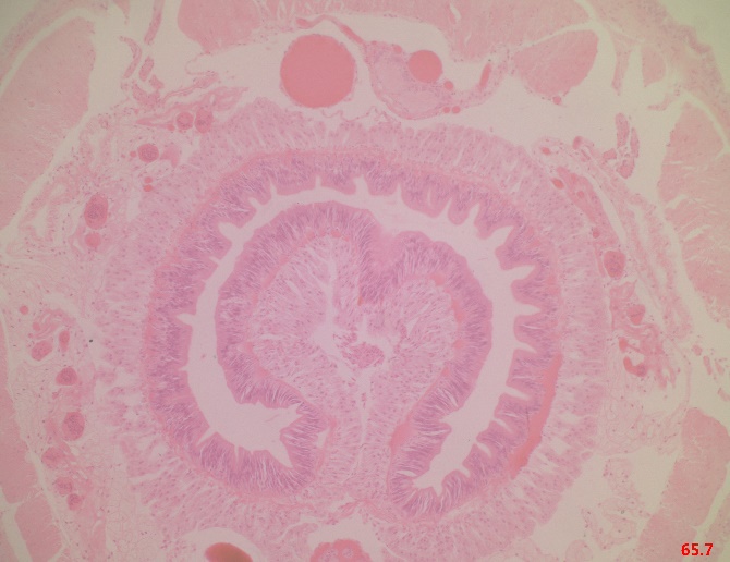
- Life Sciences: Tissue sections, entomology, live plant observation
- Education & Training: University material science virtual experiments, STEAM maker courses
Application Cases
Successful implementation experience across multiple industries
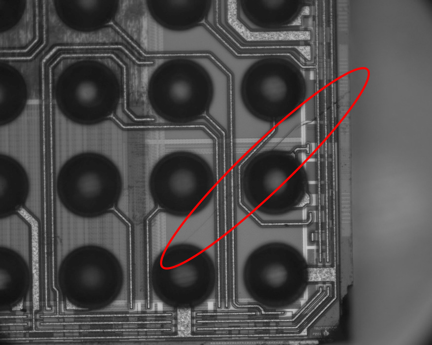
Semiconductor Manufacturing

FPC/PCB Quality Control
New Energy Materials