

FM100 Series - Fluorescence microscope system
Product Introduction
A fluorescence microscope observes fluorescent or phosphorescent specimens. Excitation light of a specific wavelength (or band) illuminates the sample; fluorophores absorb the energy and emit longer-wavelength light. Emission filters separate the emitted light from excitation light so the detector records only fluorescence. In recent years, fluorescence microscopy has become indispensable for biological research, such as visualising fluorescently labeled biomolecules.
Technical Features
Application Fields
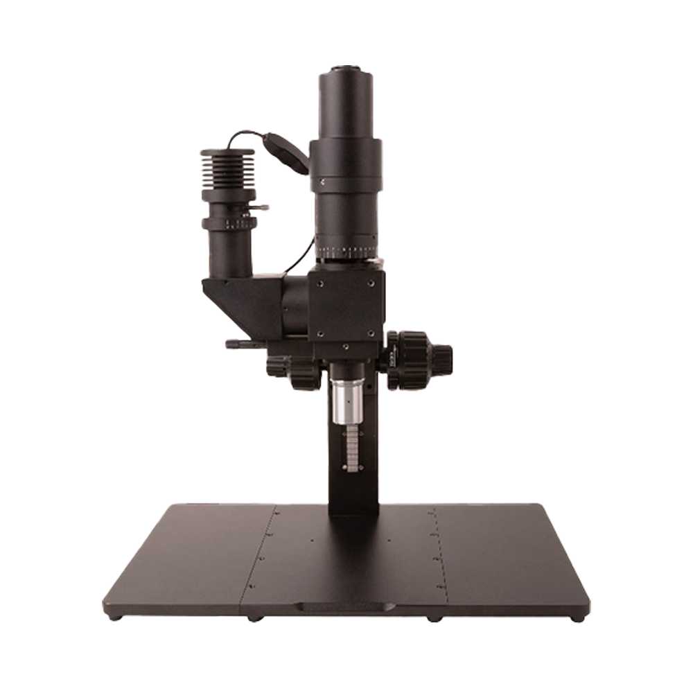
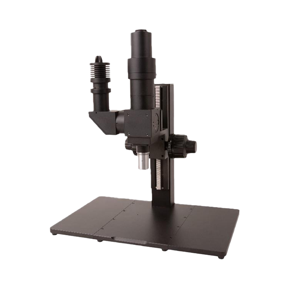
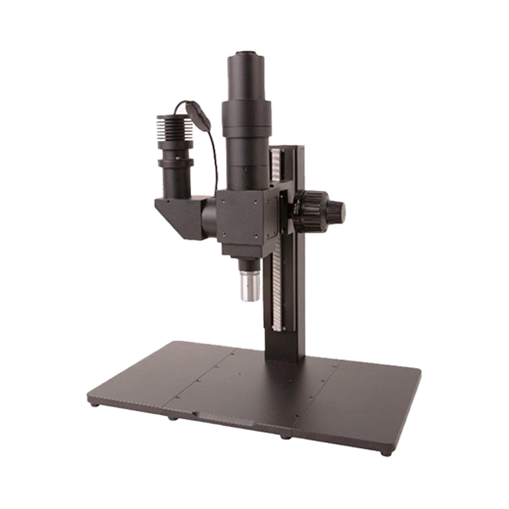
Product Details
Basic Technical Parameters
| Optical System Parameters | |
| Objective Series | Standard Working Distance Series / Long Working Distance Series (Optional) |
| Imaging Optical Path | 1X (Tube lens focal length 180 mm), customizable reduction lenses available |
| Image Plane Size | 25 mm |
| Spectral Range | Visible Light |
| Camera Interface | C/M42/M52 options available |
| Illumination System Parameters | |
| Illumination Method | Critical illumination/Kohler illumination options available |
| Light Source | 10W white light/blue light LED illumination options available |
Objective Parameters Table
Standard Working Distance Series
| Model | Magnification | Numerical Aperture (NA) | Working Distance (WD) | Focal Length | Resolution | Object Field | Image Field | Thread |
|---|---|---|---|---|---|---|---|---|
| BF5XA | 5X | 0.15 | 23.5 mm | 39 mm | 2.2 µm | 5 mm | 25 mm | M26*0.705 |
| BF10XA | 10X | 0.3 | 22.8 mm | 20 mm | 1.1 µm | 2.5 mm | 25 mm | M26*0.705 |
| BF20XA | 20X | 0.4 | 19.2 mm | 10 mm | 0.8 µm | 1.1 mm | 25 mm | M26*0.705 |
| BF50XA | 50X | 0.55 | 11 mm | 4 mm | 0.6 µm | 0.44 mm | 25 mm | M26*0.705 |
Long Working Distance Series
| Model | Magnification | Numerical Aperture (NA) | Working Distance (WD) | Focal Length | Resolution | Object Field | Image Field | Thread |
|---|---|---|---|---|---|---|---|---|
| BFL2XA | 2X | 0.055 | 33.7 mm | 100 mm | 6.1 µm | 12.5 mm | 25 mm | M26*0.705 |
| BFL5XA | 5X | 0.14 | 33.6 mm | 40 mm | 2.2 µm | 5 mm | 25 mm | M26*0.705 |
| BFL10XA | 10X | 0.28 | 33.4 mm | 20 mm | 1.2 µm | 2.5 mm | 25 mm | M26*0.705 |
| BFL20XA | 20X | 0.34 | 29.5 mm | 10 mm | 0.8 µm | 1.25 mm | 25 mm | M26*0.705 |
| BFL50XA | 50X | 0.5 | 18.9 mm | 4 mm | 0.7 µm | 0.5 mm | 25 mm | M26*0.705 |
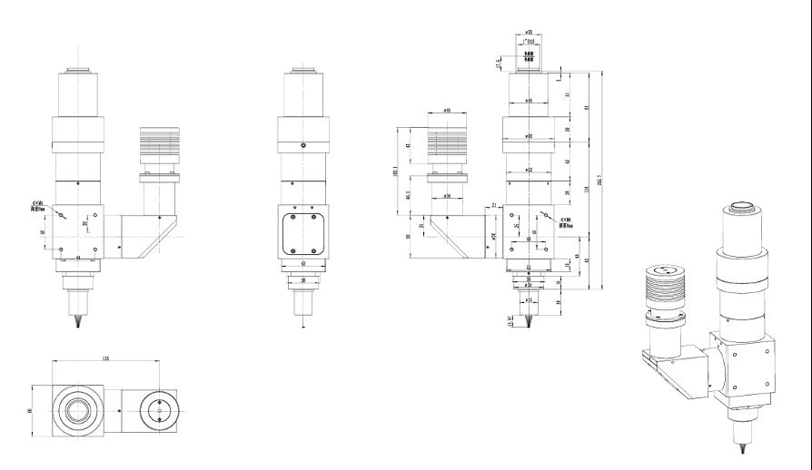
Product Dimensional Drawing
System Configuration Solutions
Flexible combination of hardware and software modules based on application requirements
| Dimension | Key Configuration | Technical Highlights | User Benefits |
|---|---|---|---|
| Imaging Hardware |
• ToupCam X Series: IMX415/IMX571 back-illuminated CMOS, up to 45 MP, USB 3.0/HDMI 60
fps 4K • HCAM/PUM Portable Module: UVC plug-and-play, built-in 8 LED ring light |
• Low read noise & 66 dB+ dynamic range • Progressive scan + optional global shutter |
True color reproduction, high contrast; suitable for high-speed AOI, fluorescence weak signal detection and multiple scenarios |
| Zoom Optics |
• MZO Series (0.25×–8×): 20× zoom ratio, NA 0.12, 174 mm long working distance • ZOPE Integrated System: Built-in 8 LED & USB camera, parfocal linear zoom |
Dual-ended parallel optical path, diffraction-limited MTF, low distortion | Zooming without refocusing, transitioning samples from millimeter to micrometer scale |
| Illumination System |
• TZM0756DRL 65/85 mm LED ring light: PWM continuously adjustable brightness • TZM0756CL coaxial light + point light source • AALRL-200 large ring light: 300 mm uniform field of view |
Multi-channel/polarized/coaxial composite light; LED angle 30° adjustable | Solving PCB solder joint glare, wafer scratches, transparent film inspection and other challenges |
| Mechanical Platform |
• TPS-600 coarse and fine adjustment stand (5 kg load capacity) • TPS-300 precision fine adjustment 2 µm step • Motorized Z & XY platforms (optional) |
Anodized Class II aerospace aluminum, ball screw | Long-term 24×7 stable positioning, supporting autofocus and array scanning |
| Software & Algorithms |
• ToupView: Real-time measurement/annotation, depth compositing, HDR, polarization
demodulation • SDK/API: Windows/macOS/Linux/Android • AI Module: Defect classification, dimensional tolerance determination |
Secondary development + PLC/robot serial protocols | Rapid integration into MES/SPC quality systems, supporting edge computing and cloud synchronization |
System Advantages
Five core advantages building professional microscopy imaging platforms
Complete Ecosystem, Turnkey Delivery
Cameras, lenses, illumination, stands, and software all developed in-house. No need for multi-vendor procurement coordination, plug-and-play saves 60% integration time.
High Resolution + Large Depth of Field
45 MP ultra-clear CMOS + depth compositing algorithms provide micrometer-level depth-clear images within 30 mm field of view.
Multi-band & Low-Light Imaging
Supports white light, near-infrared, and polarization combinations with synchronized exposure of coaxial and ring lights; presents texture details even at 0.05 lux.
Flexible Expansion, Investment Protection
Standard C-Mount and GigE Vision/USB3 Vision protocols enable later upgrades to AI modules, automated stages, and multi-camera synchronization without replacing the main system.
Cross-Industry Implementation Cases
Application Cases
Successful implementation experience across multiple industries

Semiconductor Manufacturing

FPC/PCB Quality Control

New Energy Materials
