

BMM100 Series - Brightfield metallographic microscope system
Product Introduction
A brightfield metallographic microscope is a precision optical instrument composed of illumination, imaging, and mechanical subsystems. It is widely applied across modern science and technology and serves as a critical inspection tool. Metallographic microscopes play an increasingly important role in biology, geology, mining, medicine, and related disciplines.
Technical Features
Application Fields
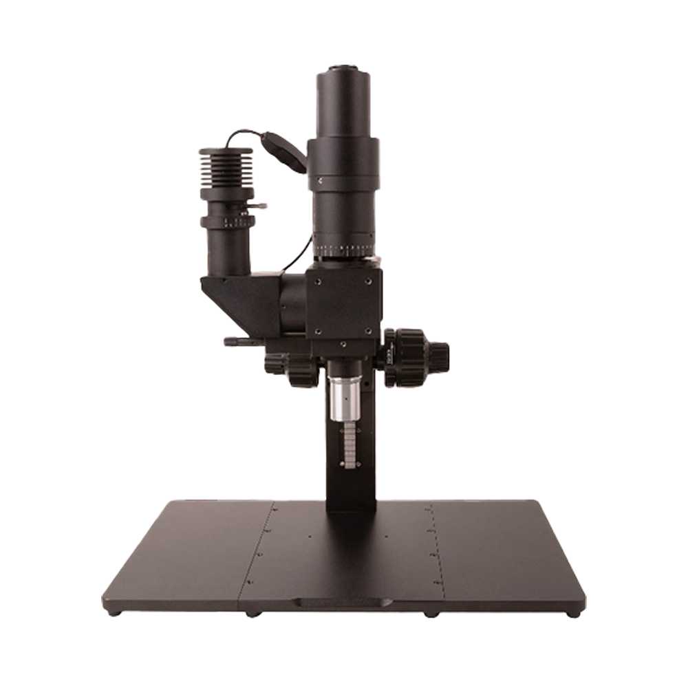
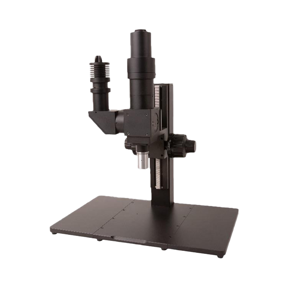
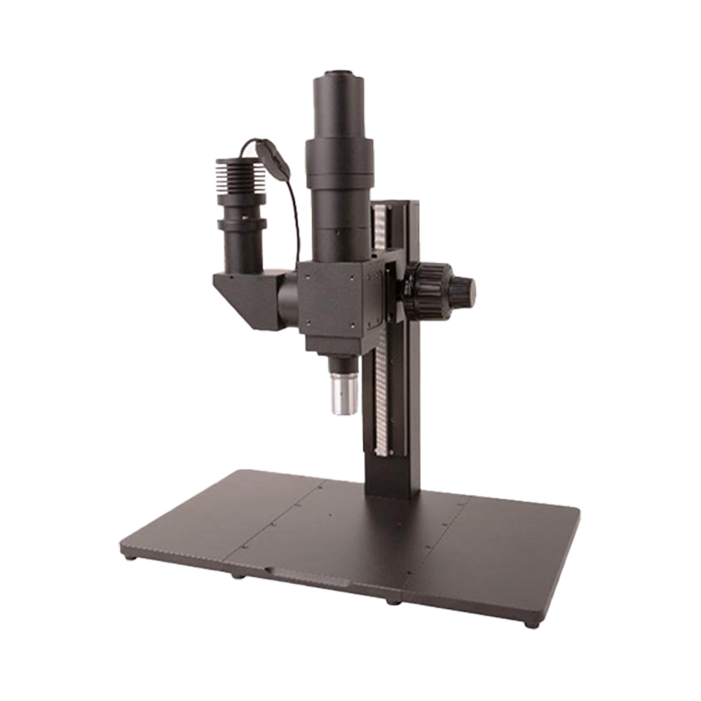
Product Details
Basic Technical Parameters
| Optical System Parameters | |
| Objective Series | Standard Working Distance Series / Long Working Distance Series (Optional) |
| Imaging Optical Path | 1X (Tube lens focal length 180 mm), customizable reduction lenses available |
| Image Plane Size | 25 mm |
| Spectral Range | Visible Light |
| Camera Interface | C/M42/M52 options available |
| Illumination System Parameters | |
| Illumination Method | Critical illumination/Kohler illumination options available |
| Light Source | 10W white light/blue light LED illumination options available |
Objective Parameters Table
Standard Working Distance Series
| Model | Magnification | Numerical Aperture (NA) | Working Distance (WD) | Focal Length | Resolution | Object Field | Image Field | Thread |
|---|---|---|---|---|---|---|---|---|
| BF5XA | 5X | 0.15 | 23.5 mm | 39 mm | 2.2 µm | 5 mm | 25 mm | M26*0.705 |
| BF10XA | 10X | 0.3 | 22.8 mm | 20 mm | 1.1 µm | 2.5 mm | 25 mm | M26*0.705 |
| BF20XA | 20X | 0.4 | 19.2 mm | 10 mm | 0.8 µm | 1.1 mm | 25 mm | M26*0.705 |
| BF50XA | 50X | 0.55 | 11 mm | 4 mm | 0.6 µm | 0.44 mm | 25 mm | M26*0.705 |
Long Working Distance Series
| Model | Magnification | Numerical Aperture (NA) | Working Distance (WD) | Focal Length | Resolution | Object Field | Image Field | Thread |
|---|---|---|---|---|---|---|---|---|
| BFL2XA | 2X | 0.055 | 33.7 mm | 100 mm | 6.1 µm | 12.5 mm | 25 mm | M26*0.705 |
| BFL5XA | 5X | 0.14 | 33.6 mm | 40 mm | 2.2 µm | 5 mm | 25 mm | M26*0.705 |
| BFL10XA | 10X | 0.28 | 33.4 mm | 20 mm | 1.2 µm | 2.5 mm | 25 mm | M26*0.705 |
| BFL20XA | 20X | 0.34 | 29.5 mm | 10 mm | 0.8 µm | 1.25 mm | 25 mm | M26*0.705 |
| BFL50XA | 50X | 0.5 | 18.9 mm | 4 mm | 0.7 µm | 0.5 mm | 25 mm | M26*0.705 |
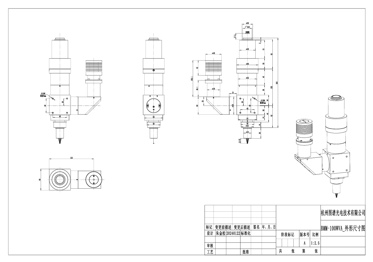
Product Dimensional Drawing
System Configuration Solutions
Flexible combination of hardware and software modules based on application requirements
| Dimension | Key Configuration | Technical Highlights | User Benefits |
|---|---|---|---|
| Imaging Hardware |
• ToupCam X Series: IMX415/IMX571 back-illuminated CMOS, up to 45 MP, USB 3.0/HDMI 60
fps 4K • HCAM/PUM Portable Module: UVC plug-and-play, built-in 8 LED ring light |
• Low read noise & 66 dB+ dynamic range • Progressive scan + optional global shutter |
True color reproduction, high contrast; suitable for high-speed AOI, fluorescence weak signal detection and multiple scenarios |
| Zoom Optics |
• MZO Series (0.25×–8×): 20× zoom ratio, NA 0.12, 174 mm long working distance • ZOPE Integrated System: Built-in 8 LED & USB camera, parfocal linear zoom |
Dual-ended parallel optical path, diffraction-limited MTF, low distortion | Zooming without refocusing, transitioning samples from millimeter to micrometer scale |
| Illumination System |
• TZM0756DRL 65/85 mm LED ring light: PWM continuously adjustable brightness • TZM0756CL coaxial light + point light source • AALRL-200 large ring light: 300 mm uniform field of view |
Multi-channel/polarized/coaxial composite light; LED angle 30° adjustable | Solving PCB solder joint glare, wafer scratches, transparent film inspection and other challenges |
| Mechanical Platform |
• TPS-600 coarse and fine adjustment stand (5 kg load capacity) • TPS-300 precision fine adjustment 2 µm step • Motorized Z & XY platforms (optional) |
Anodized Class II aerospace aluminum, ball screw | Long-term 24×7 stable positioning, supporting autofocus and array scanning |
| Software & Algorithms |
• ToupView: Real-time measurement/annotation, depth compositing, HDR, polarization
demodulation • SDK/API: Windows/macOS/Linux/Android • AI Module: Defect classification, dimensional tolerance determination |
Secondary development + PLC/robot serial protocols | Rapid integration into MES/SPC quality systems, supporting edge computing and cloud synchronization |
System Advantages
Five core advantages building professional microscopy imaging platforms
Complete Ecosystem, Turnkey Delivery
Cameras, lenses, illumination, stands, and software all developed in-house. No need for multi-vendor procurement coordination, plug-and-play saves 60% integration time.
High Resolution + Large Depth of Field
45 MP ultra-clear CMOS + depth compositing algorithms provide micrometer-level depth-clear images within 30 mm field of view.
Multi-band & Low-Light Imaging
Supports white light, near-infrared, and polarization combinations with synchronized exposure of coaxial and ring lights; presents texture details even at 0.05 lux.
Flexible Expansion, Investment Protection
Standard C-Mount and GigE Vision/USB3 Vision protocols enable later upgrades to AI modules, automated stages, and multi-camera synchronization without replacing the main system.
Cross-Industry Implementation Cases
Application Cases
Successful implementation experience across multiple industries

Semiconductor Manufacturing

FPC/PCB Quality Control

New Energy Materials
