300–1700 nm | China-made SWIR CQD (Quantum Dot) | USB3 | Cooled | Short-Wave Infrared Camera
Product Introduction
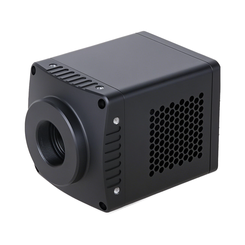
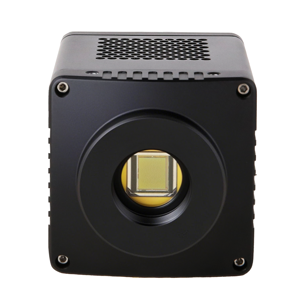
The CQD series cooled Short-Wave Infrared (SWIR) camera employs an innovative quantum dot material sensor, breaking through traditional InGaAs limitations to achieve a 300-1700 nm ultra-wide spectral response. Integrated with a deep TEC cooling system, it significantly enhances low-light and long-exposure imaging capabilities. Supporting a USB 3.0 high-speed interface, it features high sensitivity, low noise, global shutter, and rich IO interfaces, widely applied in scientific research, medical imaging, semiconductor inspection, and other innovative fields.
Product Features
- 300-1700 nm wide-spectrum CQD quantum dot sensor
- Deep TEC cooling design, low noise performance
- High sensitivity, global shutter
- USB 3.0 high-speed data interface
- High frame rate and multi-platform SDK support
- Rich IO interfaces, supporting external triggering
- 4 Gb memory
- Support for on-site firmware upgrades and OEM customization
Product Models
Optional 800–1700 / 400–1700 | CQD Series | USB 3.0 Cooled 300–1700 nm Quantum Dot SWIR Camera
| Product Model | Sensor | Resolution | Pixel Size | Spectral Range | Frame Rate | Data Interface | Dynamic Range | Actions |
|---|---|---|---|---|---|---|---|---|
| SWIR334KMB-U110 |
China-made 640×512 (CQDs)
9.60 mm × 7.68 mm
|
0.33 MP (640×512) | 15 µm × 15 µm |
800–1700 nm
|
8/12/14 Bit: 110 fps @ 640×512
|
USB3 |
71.6 dB
|
View Details |
| SWIR335KMB-U200 |
China-made 640×512 (CQDs)
9.60 mm × 7.68 mm
|
0.33 MP (640×512) | 15 µm × 15 µm |
400–1700 nm
|
200 fps @ 640×512
|
USB3 |
-
|
View Details |
Quantum Efficiency Curve #
Typical quantum efficiency response for the 300–1700 nm CQD cooled model
SWIR334 (800–1700 nm)

SWIR335 (400–1700 nm)

The official curve charts are for illustrative purposes only and show typical quantum efficiency versus wavelength. SWIR334 response range: 800–1700 nm; SWIR335 response range: 400–1700 nm.
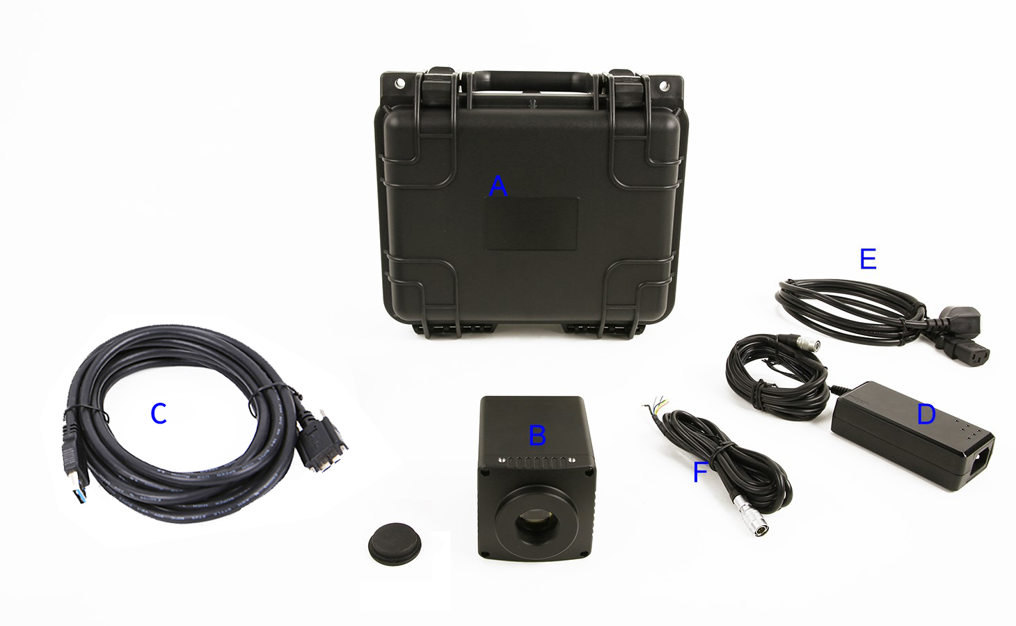
Packing List #
Standard configuration and packing details for the 300–1700 nm CQD series (USB3 · deep cooling)
- A 3-A instrument safety case: L: 28 cm W: 23.0 cm H: 15.5 cm (1 pc, ≈2.8 kg/box)
- B CQD 300–1700 USB interface camera
- C High-speed USB3 A-to-B gold-plated data cable (1.5 m)
- D 12 V / 3 A 6-pin aviation connector power adapter
- E Power cord
- F External trigger control cable (1 pc)
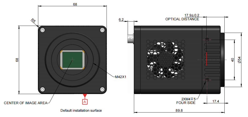
Product Dimensions #
Outline drawing of the USB3 cooled model (C-mount)
Frequently Asked Questions
Learn more about CQD SWIR colloidal quantum dot short-wave infrared camera technology
Deep Understanding of CQDs CMOS SWIR Cameras
CQDs CMOS image sensors are a new type of short-wave infrared (SWIR) imaging technology that uses Colloidal Quantum Dots as photosensitive materials and deeply integrates with standard CMOS processes. Compared to traditional InGaAs solutions, CQDs CMOS sensors offer advantages such as high cost-effectiveness, high resolution, compact size, suitability for large-scale mass production, and environmental friendliness, promoting SWIR imaging from high-end scientific research to broader industrial, agricultural, and consumer-level applications.
The absorption peak of CQDs materials can be flexibly customized by adjusting quantum dot particle sizes, enabling a single chip to cover a broad wavelength band from approximately 300–1700 nm or even extended to 2500 nm. Their quantum efficiency, dynamic range, and signal-to-noise ratio continue to improve, with some models capable of room temperature low-noise imaging and optional TEC cooling for high-requirement scenarios.
CQDs CMOS SWIR cameras feature standard optical interfaces and compact module designs for easy system integration and large-scale applications, making them ideal solutions for industrial inspection, material analysis, semiconductors, agricultural sorting, machine vision, food and pharmaceutical testing, and other fields.
Technical Features
Core advantages of CQDs CMOS SWIR technology
Wide Spectral Tuning Capability
By selecting different CQDs materials and particle sizes, sensitive response across 300–1700 nm or even broader wavelength bands can be customized to meet diverse application requirements.
High Cost-Effectiveness
Using standard CMOS large-scale manufacturing, unit costs are significantly lower than InGaAs solutions, suitable for batch integration and consumer-level applications.
High Resolution and Small Pixels
Supports high pixel density designs with fine image quality, facilitating detection of minute defects and details, improving inspection accuracy.
Room Temperature/Cooled Dual Mode
Supports room temperature low-noise imaging and optional TEC cooling for high-end scenario requirements, offering strong adaptability.
Environmentally Friendly
New-generation CQDs materials (such as Ag₂Te, InAs, etc.) comply with RoHS standards, meeting global market green compliance requirements.
Flexible and Easy Integration
Compact size and low power consumption, suitable for embedded devices and various intelligent terminal systems with high integration levels.
Application Scenarios
Wide application fields for CQDs CMOS SWIR cameras
Machine Vision and Industrial Inspection
Applied in semiconductor defect detection, plastic/food/pharmaceutical sorting, printing inspection, and other industrial scenarios, providing high-precision quality control solutions.
Complex Environment Imaging
Can still obtain clear images in scenarios where visible light is limited by haze, smoke, and dust, providing excellent environmental adaptability.
Material Sorting and Scientific Analysis
Suitable for precision material identification, scientific experiments, agricultural sorting, and other high-end applications, providing accurate spectral analysis capabilities.
Intelligent Sensing and Consumer Electronics
Suitable for embedding in intelligent terminals, expanding new applications such as night vision and non-invasive detection, promoting civilian adoption of SWIR technology.
Application Examples
Demonstration of CQDs CMOS SWIR camera applications in real-world scenarios


More Application Industry References
- Semiconductor Industry: Solar cell and chip inspection
- Agriculture: Spectral remote sensing applications via multirotor aircraft
- Recycling Industry: Material sorting of plastics, waste, and other materials
- Medical Imaging and Research: Hyperspectral and multispectral imaging
- Food Industry: Quality inspection and grading
- Beverage Industry: Liquid level detection in opaque containers
- Packaging: Seal inspection
- Glass Industry: High-temperature glass penetration defect detection
- Printing Industry: See-through hidden features
- Video Surveillance: Visual enhancement (e.g., smoke penetration)
- Security: Counterfeit detection, such as currency, wigs, or skin