Semiconductor
SWIR Camera Applications in Solar Panel Production Lines
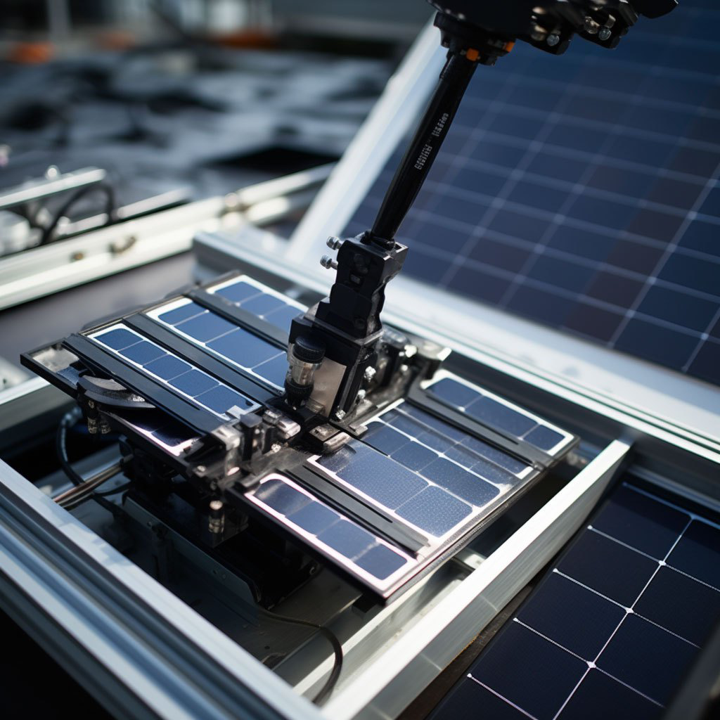
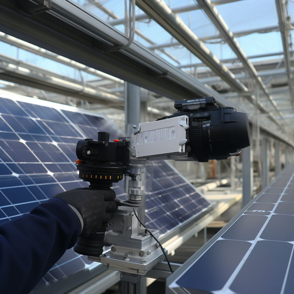
Quality inspection in semiconductor equipment production lines represents a critical task that ensures product quality assurance. Short-Wave Infrared (SWIR) machine vision cameras play an important role in this context. These specialized cameras can capture infrared light invisible to the human eye, enabling them to detect numerous issues that traditional optical systems might overlook.
Solution Background:
Quality inspection in solar panel production lines represents a critical task for ensuring product quality. SWIR series machine vision cameras play an important role in this application. These specialized cameras can capture infrared light invisible to the human eye, enabling them to detect numerous issues that traditional optical systems might overlook. These cameras employ dual noise reduction technology, featuring ultra-high sensitivity and low noise characteristics.
Advantages of Implementing SWIR Cameras in Production Lines:
Defect Detection: SWIR cameras can detect minute physical defects such as scratches, cracks, particles, or delaminated layers. These defects are crucial for flaw identification and early intervention.
Solder Joint Detection: Due to the SWIR camera's spectral range extending from 1.0 to 1.7 µm, they can detect minute solder joints in semiconductors. Small solder joint cracks or defective joints can be identified, which is often impossible to accomplish with traditional visual inspection solutions.
Lead Wire and Chip Detection: SWIR cameras possess sufficient resolution to inspect micrometer-level lead wires and chips. Lead wire arrangement, chip positioning, and dimensions can all be rapidly and accurately detected.
Depth Imaging: SWIR cameras can also determine depth information under different materials, enabling depth positioning and analysis of multi-layer components and complex solder joints in circuit boards.
Non-Destructive Testing: Through the use of SWIR cameras, non-destructive testing of materials can be performed. This means that during the inspection process, no physical changes occur to the tested materials or their performance characteristics.
Application Value:
The importance of all these quality inspections lies in enabling semiconductor manufacturing companies to detect and correct errors early, thereby saving costs, improving product quality, and reducing time-to-market.


