sNIRII640B-U3 Scientific Camera
Product Introduction
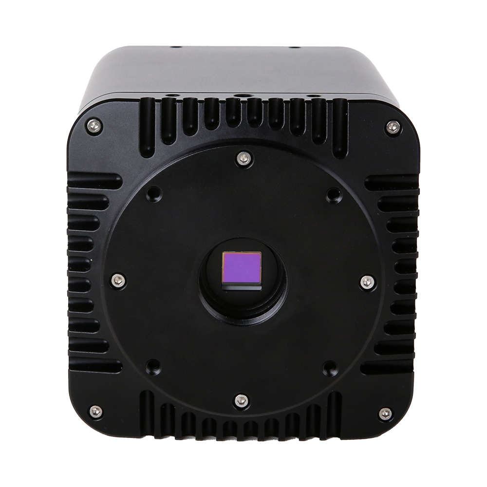
The sNIRII series targets cutting-edge research applications in the 900–1700 nm (NIR-II) spectral range, employing China-made InGaAs image sensors that combine high sensitivity with low readout noise, suitable for in vivo near-infrared imaging, biological fluorescence detection, materials/device characterization, and other scenarios. The typical configuration provides 640×512 resolution with 15 µm pixels, maintaining excellent contrast and detail even under low-light conditions.
To suppress dark current and thermal noise, the system features TEC cooling with closed-loop temperature control, reducing the sensor operating temperature by approximately 40 °C below ambient; combined with anti-fogging optical design, this ensures stable and clean imaging under low temperature and long exposure conditions.
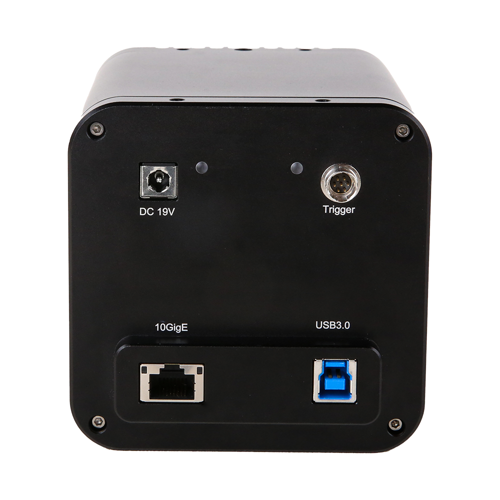
The camera provides USB3.0 and 10GigE (model-dependent) high-speed data links, supporting 8/16-bit data output with built-in buffer to ensure link stability during high-speed acquisition. Acquisition modes include free-running, software/hardware triggering, facilitating synchronization with lasers, light sources, motion/stepper platforms, and other research equipment. Complete with ToupView and cross-platform SDK (Windows/Linux, C/C++/C#/Python) for system integration and secondary development.
Key Features
- China-made InGaAs near-infrared sensor, response covering 900–1700 nm (NIR-II)
- Typical resolution 640×512, 15 µm pixels; sensor area approximately 9.6×7.68 mm (model-dependent)
- TEC cooling with closed-loop temperature control, typical ΔT ≈ 40 °C (below ambient), significantly reducing dark current
- Anti-fogging optical design, effectively suppressing condensation under low temperature and long exposure conditions
- 8/16-bit image data output, enhancing weak signal gradation and dynamic range
- Built-in 512 MB buffer, ensuring data integrity during high-speed transmission
- USB3.0 / 10GigE high-speed interface (model-dependent), meeting different platform bandwidth requirements
- Acquisition modes: free-running, software trigger, hardware trigger, facilitating timing synchronization with external equipment
- Support for ROI setting and digital binning (2×2 / 3×3 / 4×4), flexible balance between resolution/frame rate/SNR
- Power supply: 19 V independent power supply (4.74 A, model-dependent)
- Environmental adaptability: −30 to 45 °C, humidity 0–95% (non-condensing, model-dependent)
- Windows / Linux platform SDK provided, supporting C/C++, C#, Python; complete with ToupView
- Support for field firmware upgrade
- Compliant with CE / FCC / RoHS certifications (model-dependent)
Product Details
| Specifications | |
| Model | sNIRII640B-U3 |
| Sensor | China-made InGaAs image sensor |
| Shutter Type | Global shutter |
| Color Type | Monochrome |
| Resolution | 0.33MP (640×512) |
| Sensor Size | 9.6 mm × 7.68 mm |
| Sensor Diagonal | 1/2" |
| Pixel Size | 15 µm × 15 µm |
| Performance Parameters | |
| Frame Rate | TBD@640×512 |
| Bit Depth | 8/16-bit |
| Dynamic Range | 55.8 dB (HCG); 58.1 dB (MCG); 58.3 dB (LCG) |
| Sensitivity | TBD |
| Interface Parameters | |
| GPIO | 1 opto-isolated input, 1 opto-isolated output, 2 non-isolated I/O ports |
| Lens Mount | C-mount |
| Data Interface | USB3.0 |
| Power Supply | 19 V 4.74 A DC |
| Physical Parameters | |
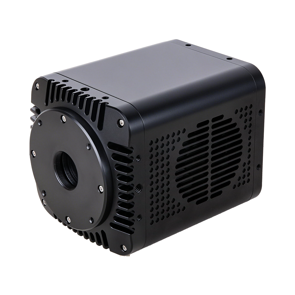
| Dimensions | 137.8 mm × 100 mm × 100 mm |
| Weight | TBD |
| Environmental Parameters | |
| Operating Temperature | −30 °C to +45 °C |
| Operating Humidity | 0-95% |
| Storage Temperature | −40 °C to +60 °C |
| Storage Humidity | 0-95% |
| Other Parameters | |
| Operating System | Windows/Linux |
| Certification | TBD |
Product Overview
sNIRII640B-U3 is a scientific-grade cooled camera featuring a China-made InGaAs image sensor back-illuminated sCMOS image sensor with the following characteristics:
- High-resolution imaging: 0.33MP (640×512) resolution, 15 µm × 15 µm pixel size, sensor format 9.6 mm × 7.68 mm
- Shutter design: Features Global shutter design, supports monochrome imaging, suitable for fluorescence imaging, spectral analysis, gene sequencing and other scientific applications
- High-speed data transmission: Supports USB3.0 high-speed data interface, maximum frame rate up to TBD@640×512 , data output formats include 8/16-bit
- Excellent dynamic range: Dynamic range up to 55.8 dB (HCG); 58.1 dB (MCG); 58.3 dB (LCG), sensitivity of TBD
- Cooling system: Built-in cooling system can reduce temperature to TBD below ambient, effectively reducing dark current
- Rich interfaces: Supports GPIO interface, lens mount is standard C-mount interface
- Compact design: Overall dimensions 137.8 mm × 100 mm × 100 mm , weight approximately TBD , power supply 19 V 4.74 A DC
- Full platform support: Supports Windows/Linux systems, includes ToupView software and cross-platform SDK, supports C/C++, C#, Python and other mainstream development languages
Core Performance Metrics
Frame Rate
Up to TBD@640×512
Resolution
0.33MP (640×512)
Dynamic Range
55.8 dB (HCG); 58.1 dB (MCG); 58.3 dB (LCG)
Scientific Imaging Features
Back-illuminated Sensor
Features back-illuminated sCMOS sensor with higher quantum efficiency, particularly suitable for weak light imaging applications
Cooling Noise Reduction
Built-in cooling system effectively reduces dark current and noise, improving image quality and signal-to-noise ratio
High Sensitivity
Sensitivity reaches TBD , meeting high-precision requirements for scientific imaging
Flexible Control
Supports ROI, binning, trigger control and other functions, adapting to different research requirements
The sNIRII640B-U3 camera, with its excellent scientific imaging performance, stable cooling system, and rich interface configuration, is an ideal choice for research institutions, medical facilities, and high-end industrial applications, capable of meeting various precision imaging and analysis requirements.
sNIRII640B-U3 Product Manual
PDF format, includes detailed technical parameters and dimensional structure
SDK Development Kit
Supports Windows, Linux, macOS and other multi-platforms
3D Model Files
STEP format, for mechanical design integration
Frequently Asked Questions
Learn more about scientific-grade CMOS camera expertise
- Ultra-low readout noise: sCMOS readout noise approaches 1e⁻, significantly better than traditional CCD
- High frame rates: Parallel readout architecture supports frame rates up to 100fps or higher
- Wide dynamic range: Can simultaneously image bright and dark regions with dynamic range reaching tens of thousands to one
- Large field of view and high resolution: Suitable for high-resolution large field of view imaging requirements
EMCCD cameras are better suited for extremely low light or long exposure applications.
sCMOS cameras offer better cost-effectiveness for high-resolution, high frame rate applications requiring low noise.
In-Depth Product Introduction
sCMOS Sensor Architecture
Each pixel is equipped with independent amplifiers and column-level ADCs, enabling parallel readout for high-speed, high signal-to-noise ratio imaging. Dual gain channels and dual ADC designs further enhance dynamic range and sensitivity.
Low Noise + Wide Dynamic Range
Typical sCMOS noise is less than 2 e⁻ at 30fps, with dynamic range reaching 50,000:1, significantly exceeding traditional CCD performance.
Fast Readout and Versatility
Parallel readout architecture supports high frame rates (greater than 100fps), suitable for high-speed event capture such as cell movement, fluorescence lifetime, plasma changes, and more.
Low Light Imaging Capability
Back-illuminated sCMOS sensors can achieve quantum efficiency greater than 95%, performing excellently from UV to near-infrared ranges, with low fixed pattern noise and cooling capabilities down to -30°C for astronomical observations.
Application Scenarios and System Value
Suitable for fluorescence microscopy, astronomical imaging, cold atom research, X-ray imaging, materials testing, industrial microscopy, and various scientific research and industrial fields, providing high sensitivity, high precision, and high adaptability system advantages.
Primary Application Areas
Applications of scientific cameras (sCMOS) across various fields


sCMOS Technical Advantages Summary
- Ultra-low readout noise (<2e⁻)
- High frame rates (>100fps)
- Wide dynamic range (50,000:1)
- High quantum efficiency (>95%)
- Large field of view high resolution
- Cooling capability (-30°C)
- Parallel readout architecture
- Multi-purpose scientific adaptability