SR Series
Product Introduction
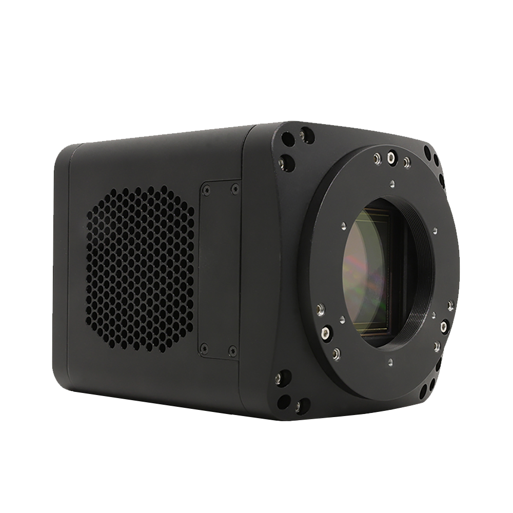
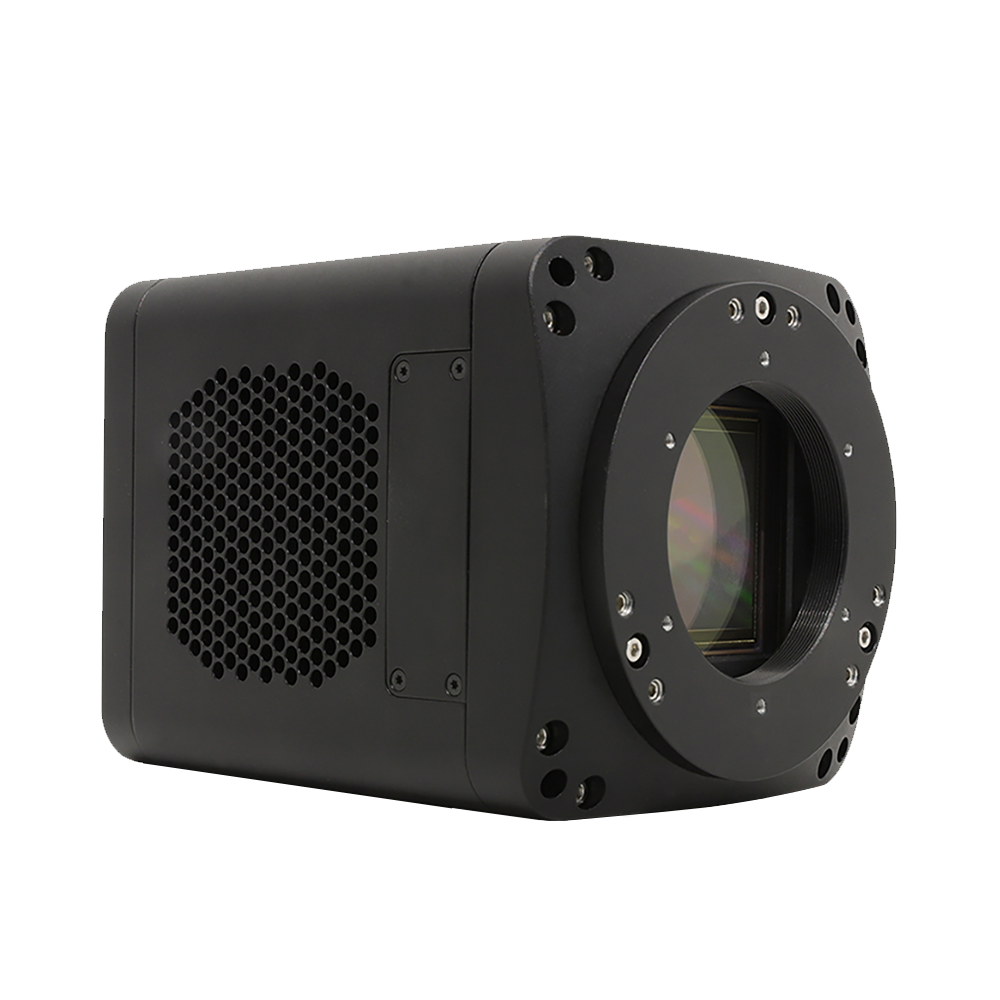
The SR series is designed for ultra-high resolution scientific imaging, utilizing the VPS2163A high-precision CMOS image sensor. It captures images at 20,480 × 27,200 (≈ 557 megapixels) with a 0.5 µm pixel size, ideal for cell morphology, biological tissue structure, semiconductor/wafer defect inspection, and microstructure metrology applications.
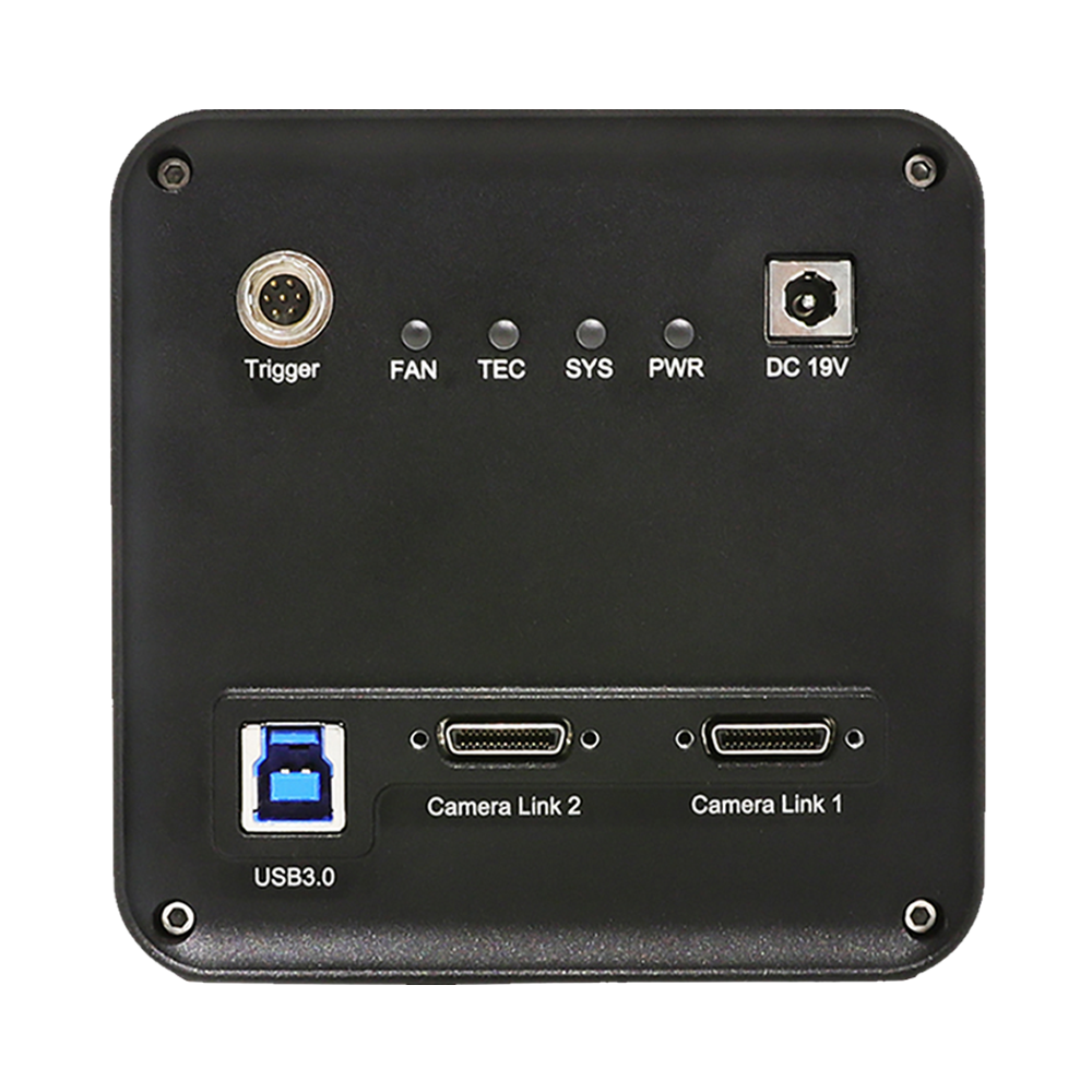
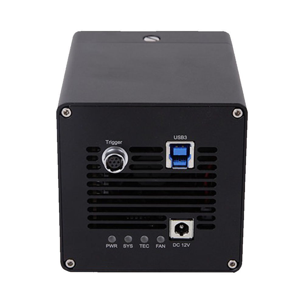
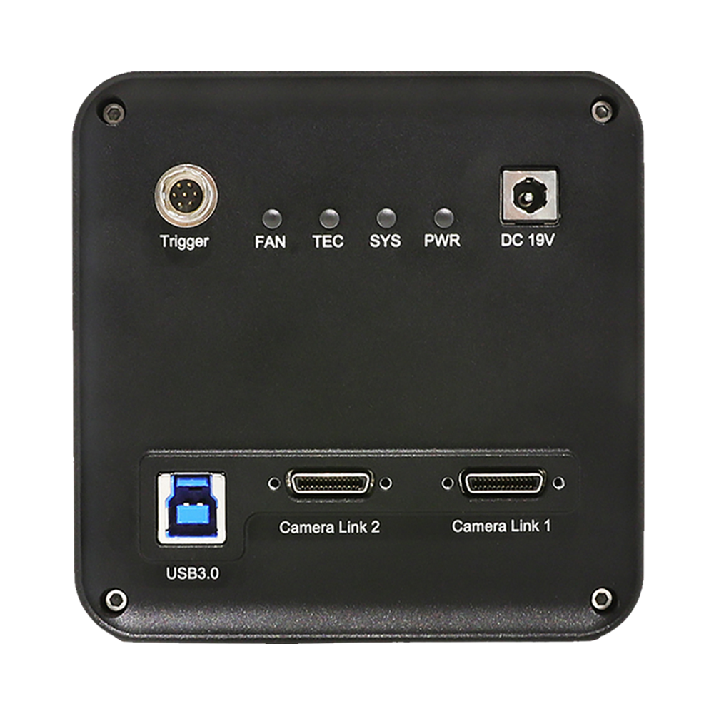
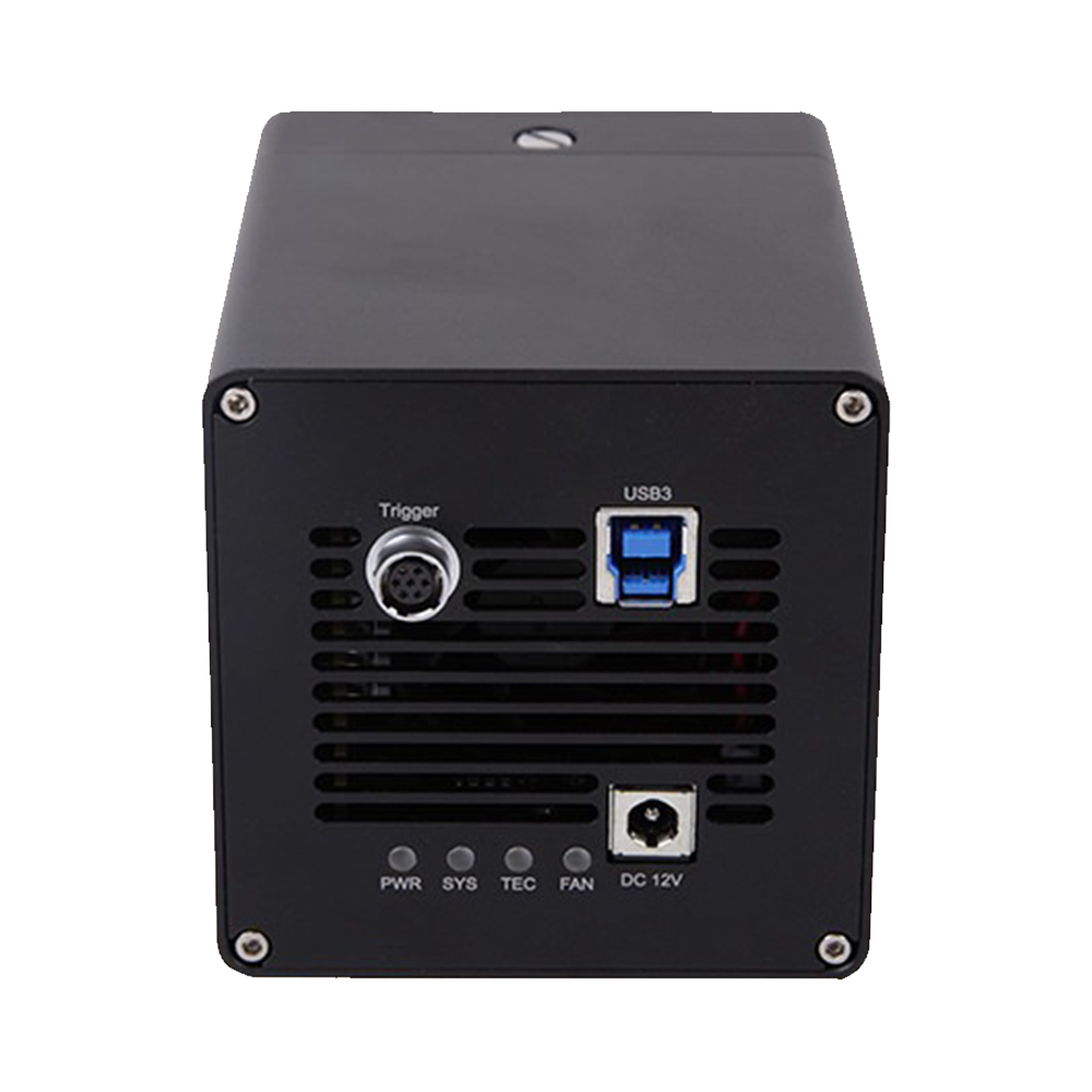
The camera features a USB 3.0 interface with 8/10-bit output formats and built-in buffer to ensure stable acquisition of large pixel images. Typical frame interval for full-resolution images is approximately 6 s (depending on acquisition and storage conditions).
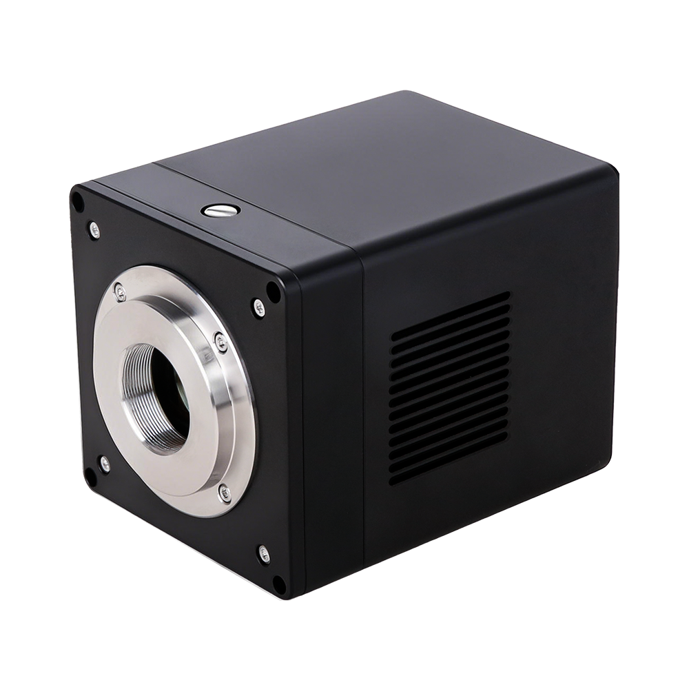
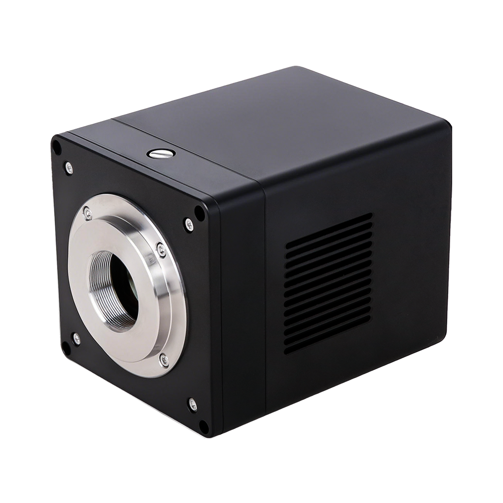
The SR series incorporates an efficient thermal control system with TEC cooling, reducing the sensor's operating temperature by about 40 °C below ambient (ΔT ≈ 40 °C). This effectively suppresses dark current and enhances consistency during long-term acquisition. The compact body supports both free-running and external triggering, compatible with various lens mounts. It comes with ToupView software and cross-platform SDK (Windows/Linux, C/C++/C#/Python) for easy system integration and custom development.
Product Features
- VPS2163A high-resolution CMOS image sensor
- Single frame resolution: 20,480 × 27,200 (≈ 557 megapixels)
- Pixel size: 0.5 µm × 0.5 µm, diagonal ≈ 17.0 mm (≈ 1.0″ optical format)
- Rolling shutter operation mode
- Typical frame interval at full resolution: ≈ 6 s (≈ 0.17 fps, depends on acquisition and storage conditions)
- Built-in ≥ 1 GB buffer (or specified as segmented buffer) ensuring stable transfer of large pixel data
- USB 3.0 (5 Gbps) data interface
- Image data format: 8/10-bit (12-bit or higher if supported by the chip)
- TEC cooling and closed-loop temperature control, typical ΔT ≈ 40 °C (below ambient), reducing dark current
- Triggering: Free-running and external trigger
- Lens mount: C (1.1″ coverage) / F / M42 (model dependent)
- Power supply: 12 V DC adapter
- Operating environment: Recommended 0 to 40 °C (or as per final thermal design), 20% to 80% RH (non-condensing)
- Windows / Linux SDK (C/C++/C#/Python), bundled with ToupView
- Supports on-site firmware upgrades
- Compliant with CE / FCC / RoHS (model dependent)
Product Models
VPS2163A Ultra-High Resolution sCMOS | 20,480 × 27,200 (≈ 557 MP), 0.5 µm, USB 3.0, for Cytology/Histology/Wafer Defect Inspection and Ultra-Precision Imaging
| Model | Sensor / Size | Resolution | Pixel Size | Shutter | Frame Rate | Interface | Dynamic Range |
Action |
|---|---|---|---|---|---|---|---|---|
| SR557MMA |
VPS2163A (sCMOS)
1" (17.02 mm) | 10.24 mm × 13.6 mm
|
557.1 MP (20480×27200) | 0.5 µm × 0.5 µm | Rolling Shutter |
0.17 fps @ 20480×27200 (≈6 s/frame)
|
USB 3.0 (5 Gbps) |
-
|
View Details |
Frequently Asked Questions
Learn more about scientific CMOS cameras
- Ultra-low read noise: sCMOS read noise approaches 1 e⁻, far outperforming traditional CCDs.
- High frame rate: Parallel readout architecture supports 100 fps or higher.
- Wide dynamic range: Captures bright and dark regions simultaneously with ratios up to tens of thousands to one.
- Large field of view and high resolution: Suits high-resolution, wide-field imaging.
EMCCD cameras excel in ultra-low light or long-exposure conditions.
sCMOS delivers greater value for high-resolution, high-speed imaging with low noise.
In-Depth Product Overview
sCMOS Sensor Architecture
Each pixel has its own amplifier and column ADC for parallel readout, enabling high-speed, high-SNR imaging. Dual gain channels and dual ADC designs further expand dynamic range and sensitivity.
Low Noise + Wide Dynamic Range
Typical sCMOS noise is < 2 e⁻ (30 fps) with dynamic range up to 50,000:1—far exceeding traditional CCDs.
Fast Readout & Versatility
Parallel readout supports >100 fps for capturing fast events such as cell motion, fluorescence lifetime studies, and plasma dynamics.
Low-Light Performance
Back-illuminated sCMOS sensors achieve >95% QE from UV to NIR, with low fixed-pattern noise and cooling down to −30 °C for astronomy and other needs.
Application Scenarios & System Value
Ideal for fluorescence microscopy, astronomy, cold atom research, X-ray imaging, materials inspection, and industrial microscopy—delivering high sensitivity, precision, and adaptability.
Key Application Areas
Representative sCMOS applications


sCMOS Technology Advantages Summary
- Ultra-low read noise (<2 e⁻)
- High frame rate (>100 fps)
- Wide dynamic range (50,000:1)
- High quantum efficiency (>95%)
- Large FOV, high resolution
- Cooling capability (−30 °C)
- Parallel readout architecture
- Adaptable to diverse research needs