
BSM Series SWIR Modular Microscope System
Product Introduction
The evolution of CMOS sensor technology has accelerated the development of compact, high-performance digital microscopy beyond the visible spectrum. The BSM Series SWIR modular microscope extends imaging from 400-700 nm into the 900-1700 nm short-wave infrared band, combining high-sensitivity SWIR cameras, dedicated optics, and modular illumination and mechanics. It bridges conventional optical microscopy and specialised infrared imaging, delivering precise non-destructive inspection for semiconductor manufacturing, materials science, and industrial inspection while maintaining compatibility with standard glass optical systems.
Product Features
- SWIR imaging coverage across 900-1700 nm for semiconductor, material, and industrial inspection
- Optical compatibility with standard glass lens systems to reduce integration and retrofitting cost
- Silicon penetration capability for non-destructive detection of subsurface defects in silicon-based materials
- Modular architecture covering illumination, imaging, and mechanical assemblies for flexible system customisation
- Coaxial Kohler illumination with 1550 / 1400 / 1300 / 1200 nm LED sources
- Support for high NA infinity SWIR microscope objectives and dedicated M Plan Apo NIR objective series
- Compact, high-sensitivity SWIR camera integration with TEC cooling and standard C-mount interface
- Micron-level resolution with refined optical path and large NA design
- High-speed imaging support with SWIR camera options up to 400 fps at reduced resolution
- Precision CNC mechanical structure with anti-vibration design for stable automated workflows
- Scalable modular platform for wavelength, sensor, and automation expansion
- Cost-effective SWIR microscopy by leveraging existing optical platforms and illumination architectures
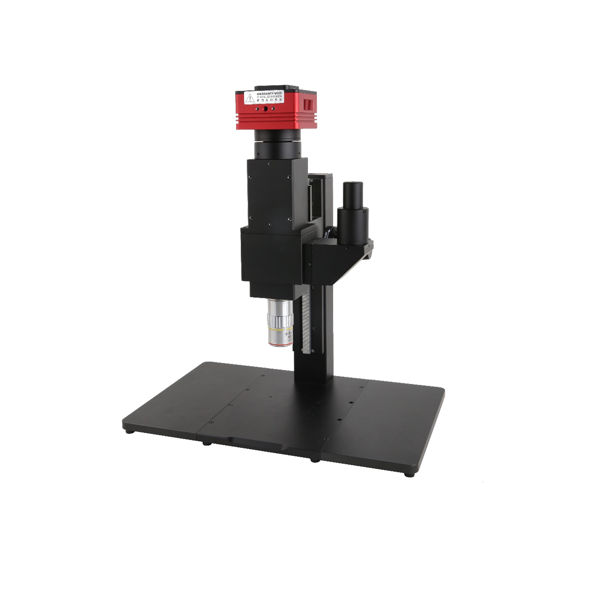
System Configuration and Parameters
Updated SWIR modular microscopy parameters for semiconductor, materials science, and industrial inspection across the 900-1700 nm waveband.
SWIR Modular Microscopy Technical Features
The BSM Series combines SWIR optical compatibility, silicon penetration capability, modular illumination, high-sensitivity imaging, and precision mechanics to deliver practical infrared microscopy on conventional microscope platforms.
Optical Compatibility
SWIR microscopy in the BSM Series works with standard glass lens systems, avoiding the reflective optics often required in MWIR and LWIR imaging and simplifying integration into conventional microscope platforms.
Silicon Penetration Capability
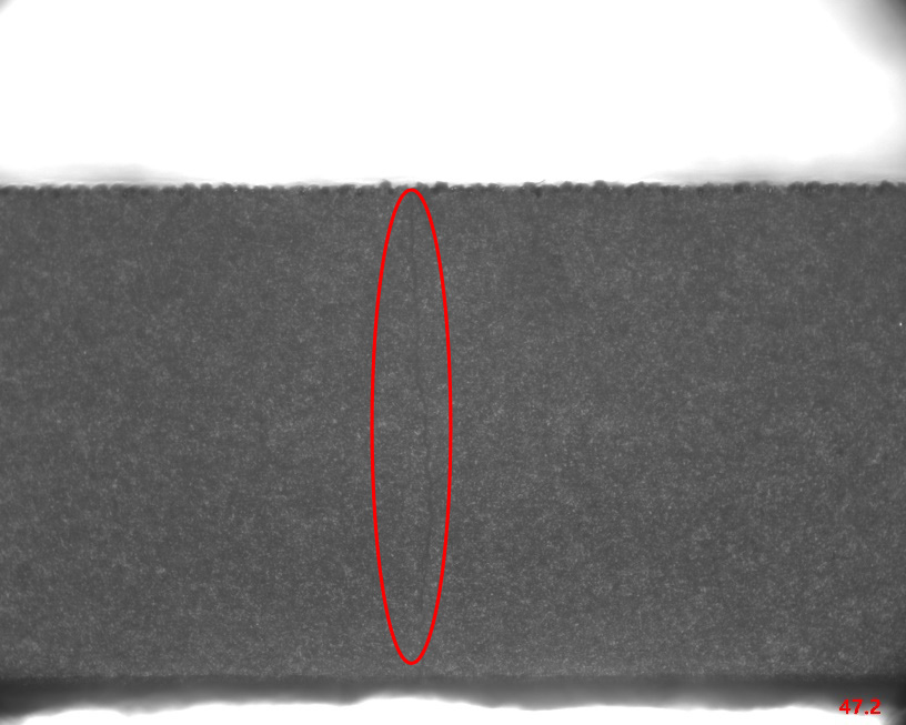
Because SWIR photon energy is below silicon's bandgap, the BSM platform can inspect internal defects in silicon-based materials such as hidden cracks in wafers, chips, and electronic interconnect structures.
Illumination and Imaging Modules
The system combines coaxial Kohler illumination, dedicated SWIR wavelengths, and high-sensitivity SWIR cameras with refined optical paths and large numerical aperture objectives for micron-level inspection.
Mechanical Module Stability
Precision CNC machining and anti-vibration structural design support stable observation and repeatable imaging in automated, continuous, or high-throughput inspection workflows.
Enhanced Material Contrast
SWIR wavelengths reveal features that are obscured in visible-light imaging, improving contrast for ceramics, composites, semiconductor structures, and other subsurface targets.
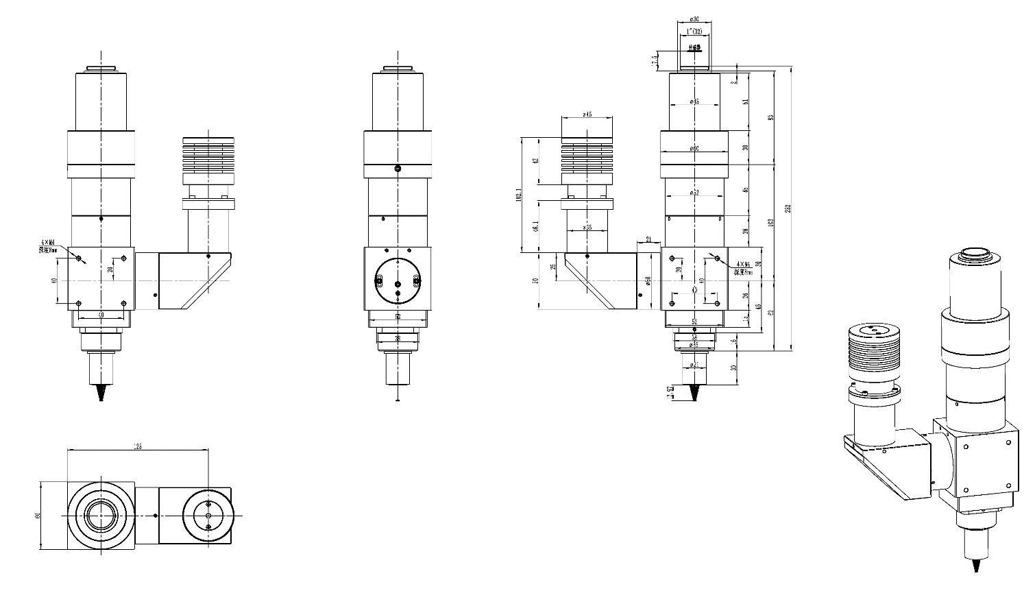
Tube Lens System Configuration
Each BSM tube lens system is now rendered from product data, making future parameter updates easier and reducing template coupling to fixed model names.
BSM-T100VA
Model: BSM-T100VA
High NA infinity SWIR objective configuration for large image circle coverage.
- Objective Support
- Support high NA infinity SWIR microscope objectives
- Tube Lens Focal Length
- 100 mm
- Field Number
- 33 mm (using 200 mm focal length tube lens)
- Wavelength
- 900-1700 nm
- Camera Interface
- C
- Illumination
- Coaxial Kohler Lighting
- Lighting Source
- 1550 / 1400 / 1300 / 1200 nm LED
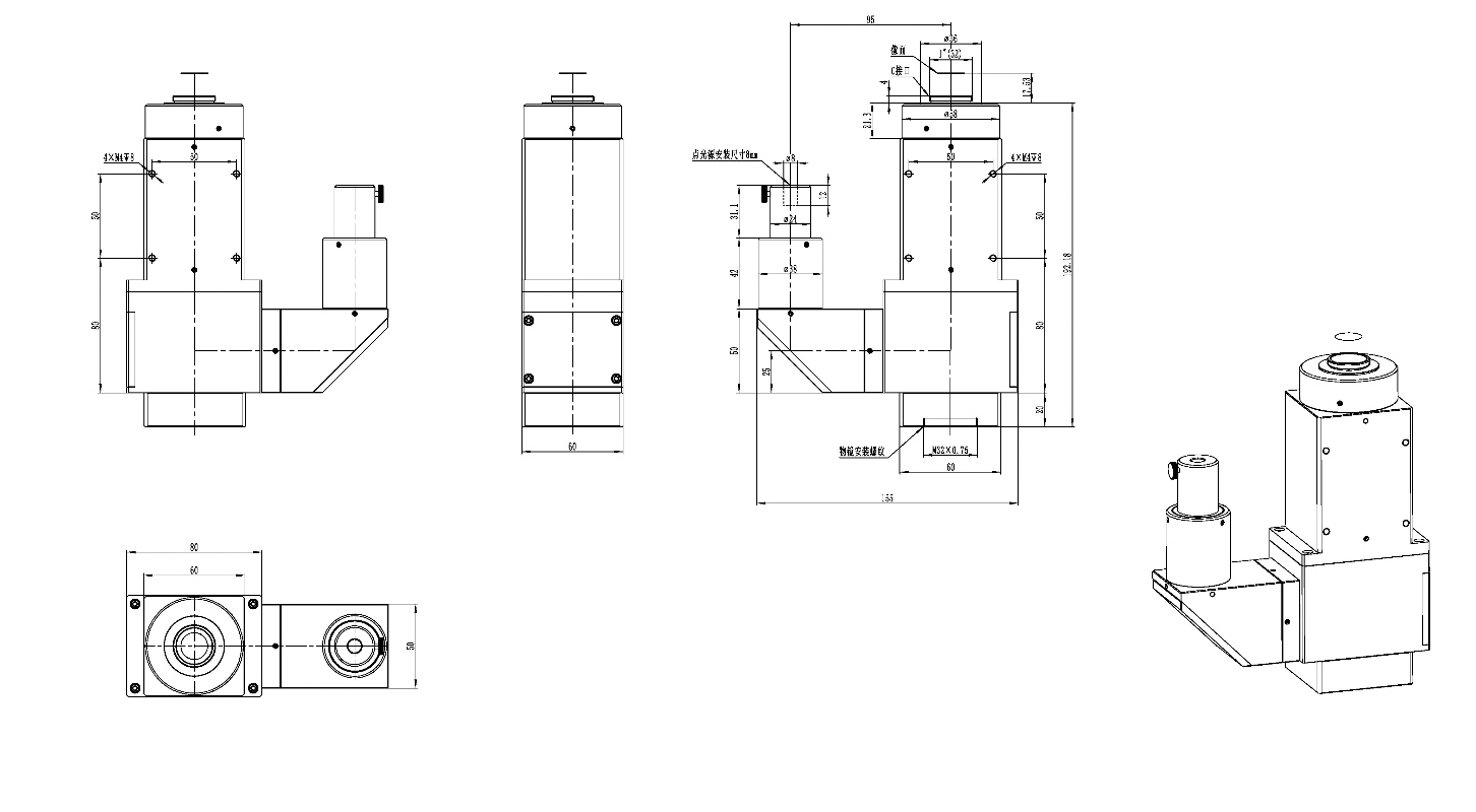
BSM-T180VB
Model: BSM-T180VB
Infinity SWIR microscope objective configuration for general-purpose SWIR inspection.
- Objective Support
- Support infinity SWIR microscope objectives
- Tube Lens Focal Length
- 180 mm
- Field Number
- 24 mm (using 180 mm focal length tube lens)
- Wavelength
- 900-1700 nm
- Camera Interface
- C
- Illumination
- Coaxial Kohler Lighting
- Lighting Source
- 1550 / 1400 / 1300 / 1200 nm LED
BSM-T090VA (Customized)
Model: BSM-T090VA (Customized)
Custom high NA infinity SWIR objective configuration with 90 mm tube lens.
- Objective Support
- Support high NA infinity SWIR microscope objectives
- Tube Lens Focal Length
- 90 mm
- Field Number
- 33 mm (using 200 mm focal length tube lens)
- Wavelength
- 900-1700 nm
- Camera Interface
- C
- Illumination
- Coaxial Kohler Lighting
- Lighting Source
- 1550 / 1400 / 1300 / 1200 nm LED
BSM-T110VA (Customized)
Model: BSM-T110VA (Customized)
Custom high NA infinity SWIR objective configuration with 110 mm tube lens.
- Objective Support
- Support high NA infinity SWIR microscope objectives
- Tube Lens Focal Length
- 110 mm
- Field Number
- 33 mm (using 200 mm focal length tube lens)
- Wavelength
- 900-1700 nm
- Camera Interface
- C
- Illumination
- Coaxial Kohler Lighting
- Lighting Source
- 1550 / 1400 / 1300 / 1200 nm LED
M Plan Apo NIR Objective Series
Updated objective parameters for SWIR microscopy applications, covering standard and high-resolution inspection from 5X to 50X HR.
| Model | Magnification | NA | WD | Focal Length | Resolution | Depth of Field | FN | Weight |
|---|---|---|---|---|---|---|---|---|
| M Plan Apo NIR 5X | 5X | 0.14 | 37.5 mm | 40 mm | 2.0 µm | 14 µm | 24 mm | 220 g |
| M Plan Apo NIR 10X | 10X | 0.26 | 30.5 mm | 20 mm | 1.1 µm | 4.1 µm | 24 mm | 250 g |
| M Plan Apo NIR 20X | 20X | 0.4 | 20 mm | 10 mm | 0.7 µm | 1.7 µm | 24 mm | 300 g |
| M Plan Apo NIR 50X | 50X | 0.42 | 17 mm | 4 mm | 0.7 µm | 1.6 µm | 24 mm | 315 g |
|
M Plan Apo NIR 50X HR High-resolution version |
50X | 0.65 | 10 mm | 4 mm | 0.4 µm | 0.7 µm | 24 mm | 450 g |
SWIR Camera Lineup
Updated SWIR camera parameters for BSM configurations, including sensor format, performance, interface, exposure range, and compact mechanical dimension.
| Model | Image Sensor | Pixel Size | Dynamic Range | SNR | Data Interface | FPS / Resolution (8bit) | Binning | Exposure Time | Dimension | TEC |
|---|---|---|---|---|---|---|---|---|---|---|
| SWIR5000KMA |
5.0M / IMX992 (M, GS) 1/1.4" (8.94 × 7.09 mm) |
3.45 × 3.45 µm | 51.5 dB | 48.5 dB | USB3 |
8 Bit: 61.9 fps @ 2560×2048, 135.7 fps @ 1280×1024
12 Bit: 35.5 fps @ 2560×2048, 135.7 fps @ 1280×1024
|
1x1
1x1
|
15 us ~ 60 s | 80 mm | Built-in TEC |
| SWIR3000KMA |
3.0M / IMX993 (M, GS) 1/1.8" (7.07 × 5.3 mm) |
3.45 × 3.45 µm | 51.5 dB | 48.5 dB | USB3 |
8 Bit: 93 fps @ 2048×1536, 176 fps @ 1024×768
12 Bit: 57 fps @ 2048×1536, 176 fps @ 1024×768
|
1x1
1x1
|
15 us ~ 60 s | 80 mm | Built-in TEC |
| SWIR1300KMA |
1.3M / IMX990 (M, GS) 1/2" (6.40 × 5.12 mm) |
5 × 5 µm | 58.7 dB | 52.6 dB | USB3 |
8 Bit: 200 fps @ 1280×1024, 392 fps @ 640×512
12 Bit: 108 fps @ 1280×1024, 209 fps @ 640×512
|
1x1
1x1
|
15 us ~ 60 s | 80 mm | Built-in TEC |
| SWIR330KMA |
0.33M / IMX991 (M, GS) 1/4" (3.20 × 2.56 mm) |
5 × 5 µm | 58.7 dB | 52.6 dB | USB3 |
8 Bit: 400 fps @ 640×512, 753 fps @ 320×256
12 Bit: 212 fps @ 640×512, 400 fps @ 320×256
|
1x1
1x1
|
15 us ~ 60 s | 80 mm | Built-in TEC |
Typical Application Cases
Professional applications of BSM system in semiconductor manufacturing, materials science, and other fields
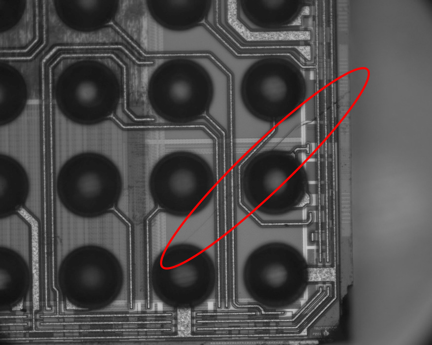
Semiconductor Manufacturing
SWIR modular microscopy supports semiconductor manufacturing by detecting subsurface defects in silicon wafers, chip interconnects, and packaged structures without destructive sample preparation.
Application Case
- Detect hidden cracks inside silicon-based chips and wafers
- Inspect interconnect integrity beneath silicon surfaces
- Support failure analysis and process quality control
- Enable non-destructive subsurface imaging for packaged devices
Materials Science
In materials science, the BSM platform identifies invisible cracks and internal structural variations in ceramics and composite materials, improving contrast for hidden defect analysis beyond visible-light microscopy.
Application Case
- Reveal hidden cracks inside ceramic structures
- Improve visibility of internal features in composite materials
- Support structural integrity and defect distribution analysis
- Provide SWIR contrast for research and material validation
More Application Fields
Industrial Inspection
The BSM modular microscope enables industrial inspection of subsurface structures and hidden defects in components without destructive disassembly, supporting quality verification and process analysis.
- Analyse subsurface structures in assembled components
- Inspect hidden defects without destructive teardown
- Support industrial quality assurance and process optimisation
Technology Advantages Comparison
| Comparison Technology | BSM System Advantages |
|---|---|
| Conventional optical microscopes | BSM systems penetrate silicon and other opaque materials to reveal internal structures, whereas conventional microscopes are limited to surface observation |
| X-ray inspection | BSM provides higher resolution, no radiation hazard, real-time imaging, and lower equipment and maintenance costs |
| Ultrasonic inspection | BSM delivers higher spatial resolution and image clarity, identifying micrometre-scale defects |
| Mid-wave / long-wave infrared systems | BSM uses standard glass optics for lower cost and better compatibility with existing microscope platforms |
System Configuration and Accessories
Standard Configuration
- BSM main system (choice of T100VA / T180VB / T090VA / T110VA)
- Multi-wavelength LED illumination module
- Coaxial Kohler illumination system
- C-mount camera adapter
- Precision focusing mechanism
Optional Accessories
- M Plan Apo NIR objective range (5X-50X HR)
- SWIR camera series (0.33M-5.0M resolution)
- Automated sample stage
- Image acquisition and analysis software
- Anti-vibration platform
- Custom-wavelength LED light sources
The BSM Series modular platform supports wavelength, camera, and automation configuration updates while staying compatible with the current optical and mechanical architecture.
BSM System Advantages
The latest BSM configuration highlights three core benefits of SWIR modular microscopy for modern inspection workflows.
Enhanced Material Contrast
SWIR wavelengths improve the visibility of structures that are difficult or impossible to distinguish in visible-light microscopy, especially for silicon, ceramics, and composite materials.
Cost Efficiency
The BSM platform uses standard microscope optics and practical LED illumination options, reducing the cost barrier compared with more specialised infrared imaging systems.
Scalability
Its modular design supports configuration changes for wavelengths, sensors, optics, and automation requirements, making the system adaptable to evolving laboratory and industrial needs.